
Inspection system and inspection image data generation method

Active Publication Date: 2015-02-12
EBARA CORP
View PDF4 Cites 4 Cited by
  • Summary
  • Abstract
  • Description
  • Claims
  • Application Information

AI Technical Summary

Benefits of technology

The patent text describes an inspection system that uses a primary optical system to shed charged particles or electromagnetic waves onto an inspection target. The system includes a movable unit that holds the target for movement, a TDI sensor that integrates the particles or waves, a position detection unit that detects the target position, and a deflector that deflects the particles or waves in a direction to compensate for any difference in position. The system can correct the position of the target to improve accuracy. The technical effects of this system include improved accuracy in inspecting the target and reduced unevenness in luminance caused by variations in exposure time.

Problems solved by technology

The generation of such unevenness in luminance leads to a reduction in inspection accuracy.

Method used


Image

  • Inspection system and inspection image data generation method
  • Inspection system and inspection image data generation method
  • Inspection system and inspection image data generation method

Examples


first embodiment

1. First Embodiment Group

[0036]According to a first embodiment of a first embodiment group, an inspection system is provided. This inspection system includes a primary optical system that sheds either of charged particles and electromagnetic waves in the form of a beam, a movable unit that can hold an inspection target to move the inspection target through a position where the beam is shed by the primary optical system in a predetermined direction, a TDI sensor that integrates amounts of secondary charged particles or electromagnetic waves that are obtained by shedding the beam on to the inspection target while the movable unit is being moved in the predetermined direction along a predetermined direction by utilizing a time delay integration system at every timing at which a transfer clock is inputted and sequentially transfers the amounts of secondary charged particles or electromagnetic waves so integrated as an integrated detection amount at every timing at which a transfer clock...

embodiment 1-a

1-A. Embodiment 1-A

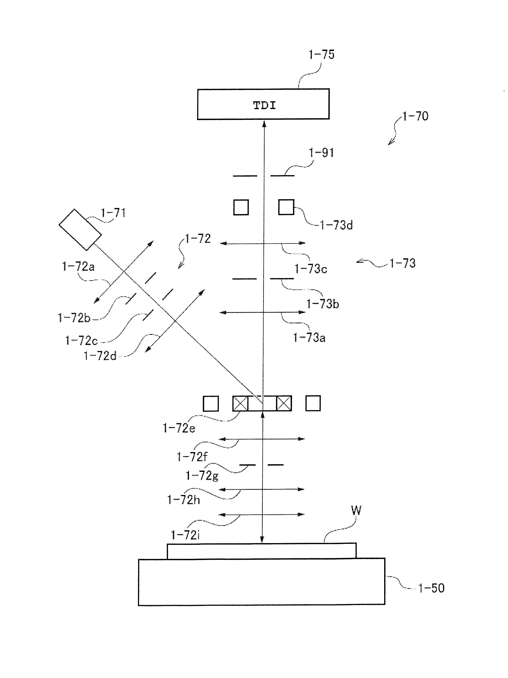
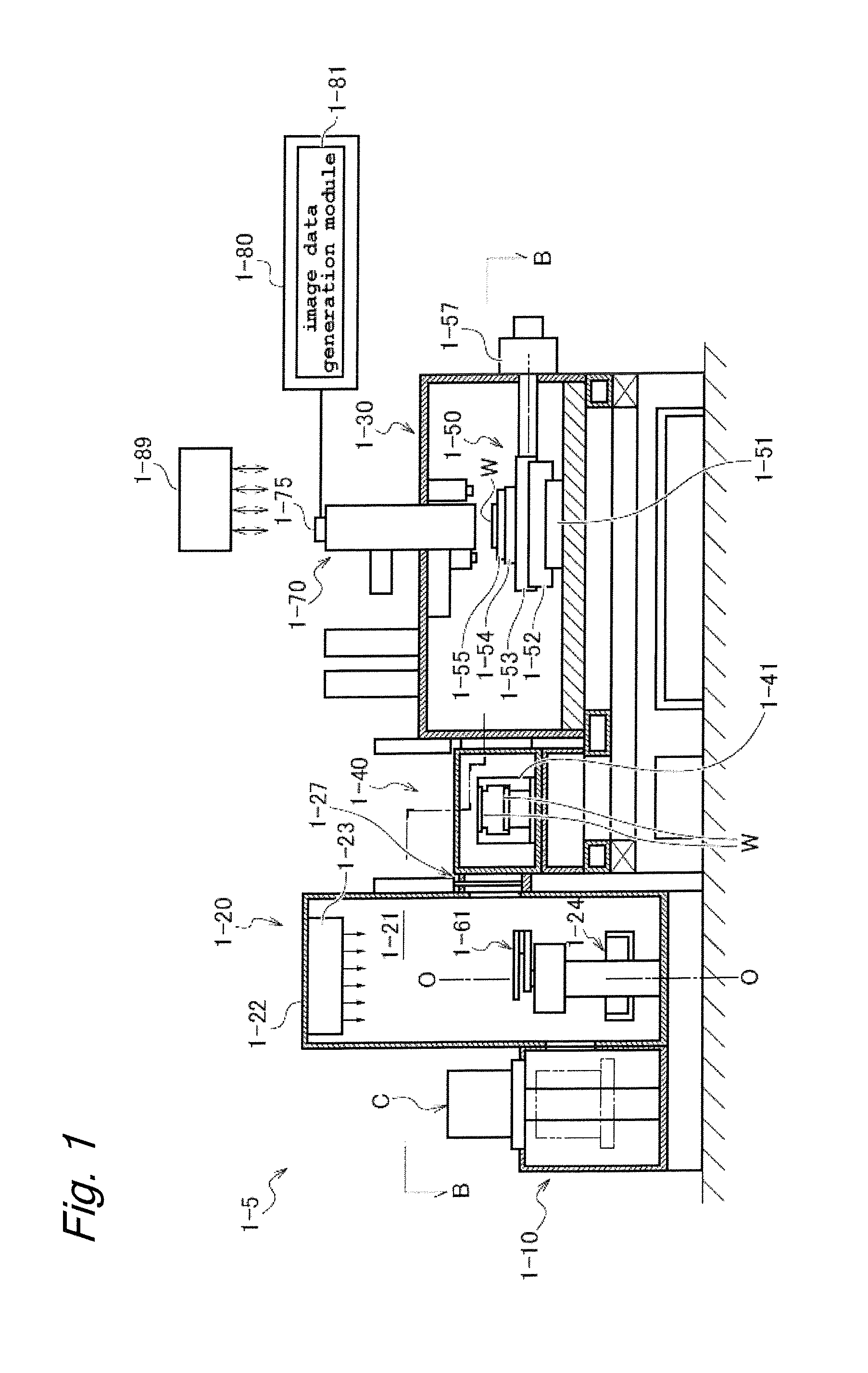
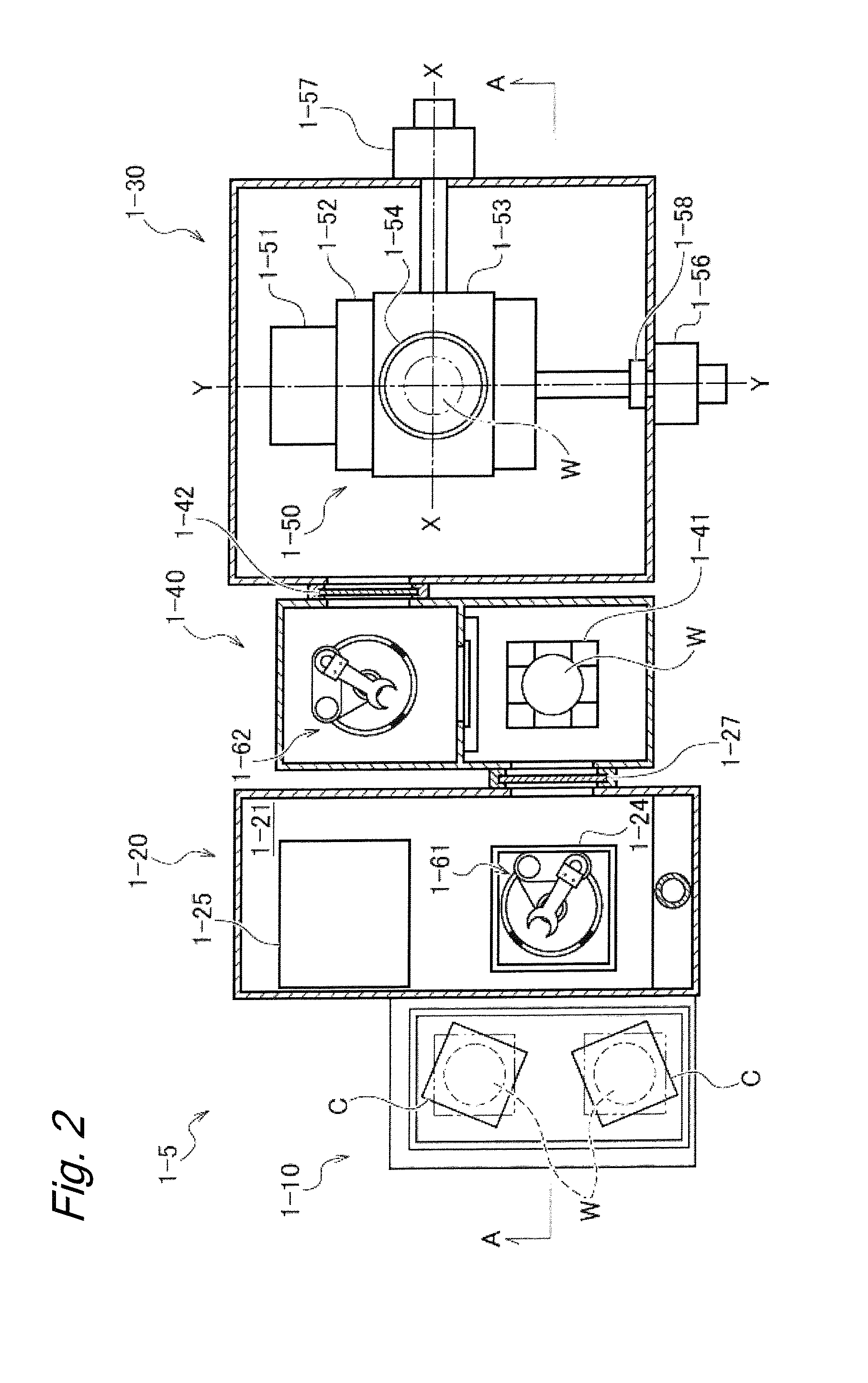
[0047]FIGS. 1 and 2 show a schematic configuration of a semiconductor inspection system (hereinafter, also referred to simply as an inspection system) 1-5 as an embodiment of an inspection system of the invention. FIG. 1 is a schematic elevation (as viewed in a direction indicated by arrows A-A in FIG. 2) of the inspection apparatus 1-5, and FIG. 2 is a schematic plan view (as viewed in a direction indicated by arrows B-B in FIG. 1) of the inspection system 1-5. The inspection system 1-5 is a system which inspects a pattern formed on a surface of an inspection target for a defect or inspects the surface of the inspection target for a foreign matter existing thereon. A semiconductor wafer, an exposure mask, an EUV mask, a nanoimprinting mask (and a template), an optic element substrate, an optical circuit substrate and the like can be raised as inspection targets. A particle, a cleaning residual (an organic matter), a reaction product on the surface and the like ca...

embodiment 1-b

1-B. Embodiment 1-B

[0079]FIG. 10 is an explanatory drawing which shows an actual position of a wafer W and a target position of the wafer W when an EO correction is executed in an embodiment 1-B. FIG. 10 corresponds to FIG. 5. In the embodiment 1-B, a transfer clock is inputted into a TDI sensor 1-75 every time the wafer W moves by a distance corresponding to one pixel in a direction Y. In this embodiment 1-B, too, a target position TP2 according to the EO correction of this embodiment is set into a step-like fashion as a whole, as shown in FIG. 10. Specifically, when looking at a specific period of time, the target position TP2 is set into a step-and-riser shape in which the target position is kept staying in the same position by a period of time which is equal to a period of time from an input of one transfer clock until an input of the following transfer clock and thereafter rises by a distance equal to one pixel of the TDI sensor 1-75 in parallel to the axis of ordinates in sync...


PUM


Abstract

An inspection system includes a TDI sensor that integrates amounts of secondary charged particles or electromagnetic waves along a predetermined direction at every timing at which a transfer clock is inputted and sequentially transfers the amounts of secondary charged particles or electromagnetic waves so integrated, and a deflector which deflects, based on a difference between an actual position and a target position of the inspection target, the secondary charged particles or electromagnetic waves directed towards the TDI sensor in a direction in which the difference is offset. The target position is set into something like a step-and-riser shape in which the target position is kept staying in the same position by a predetermined period of time that is equal to or shorter than a period of time from an input of the transfer clock to an input of the following transfer clock and thereafter rises by a predetermined distance.

Description

BACKGROUND OF THE INVENTION[0001]1. Technical Field[0002]The present invention relates to a technology for generating inspection image data for inspection of a defect or the like in a pattern formed on a surface of an inspection target by irradiating the inspection target with charged particles or electromagnetic waves.[0003]In addition, the present invention relates to a technology for generating inspection image data for inspection of a defect or the like in a pattern formed on a surface of an inspection target by irradiating the inspection target with charged particles.[0004]2. Background Art[0005]Inspection systems are widely known in which a secondary charged particle which is obtained according to the properties of a surface of an inspection target such as a semiconductor wafer or the like is detected by a TDI (Time Delay Integration) sensor by irradiating the inspection target with charged particles or electromagnetic waves, whereby a pattern or the like which is formed on th...

Claims


Application Information

Patent Timeline
IPC IPC(8): H01J37/20G01N21/64H01J37/285
CPCH01J37/20H01J2237/20228G01N21/6456H01J37/285
Inventor SUEMATSU, KENICHIYOSHIKAWA, SHOJI
Owner EBARA CORP
Features
  • Generate Ideas
  • Intellectual Property
  • Life Sciences
  • Materials
  • Tech Scout
  • Unparalleled Data Quality
  • Higher Quality Content
  • 60% Fewer Hallucinations
Learn More