Organic light emitting diode display

a light-emitting diode and display technology, applied in the field of organic light-emitting diodes (oled) display, can solve the problems of affecting the performance of the display, and affecting the appearance of the display. , to achieve the effect of improving the moisture permeation resistance and the out-gassing function, preventing or reducing the damage to the side wall of the common voltage lin

Active Publication Date: 2015-02-12
SAMSUNG DISPLAY CO LTD
View PDF10 Cites 32 Cited by
  • Summary
  • Abstract
  • Description
  • Claims
  • Application Information

AI Technical Summary

Benefits of technology

[0028]In the organic light emitting diode (OLED) display according to exemplary embodiments of the present invention, damage to the side wall of the common voltage

Problems solved by technology

However, the common voltage line may be exposed to different etching processes before forming the encapsulation member, and as a result, a side wall of the exposed common voltage line may be etched or damaged

Method used


Image

  • Organic light emitting diode display
  • Organic light emitting diode display
  • Organic light emitting diode display

Examples


Embodiment Construction

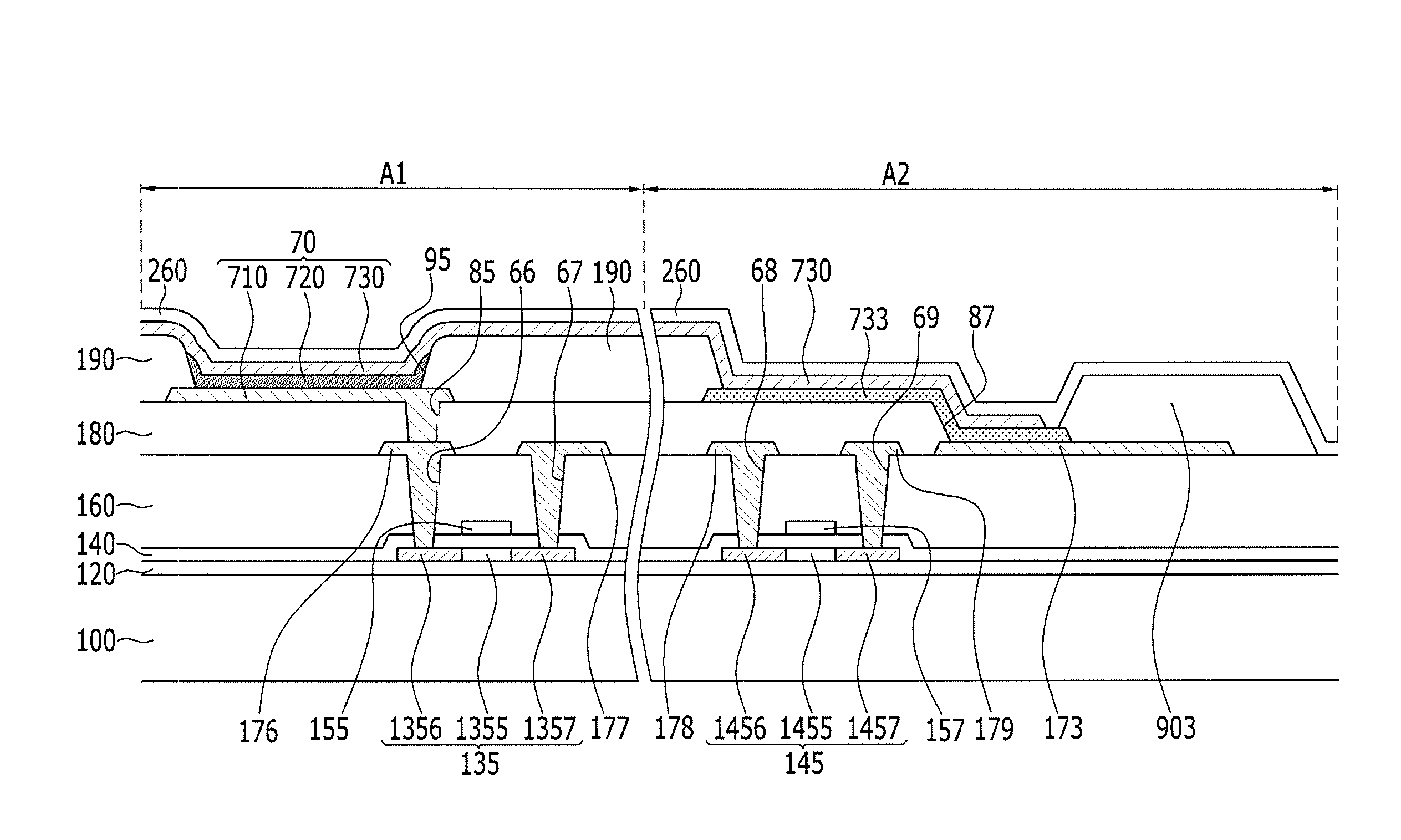
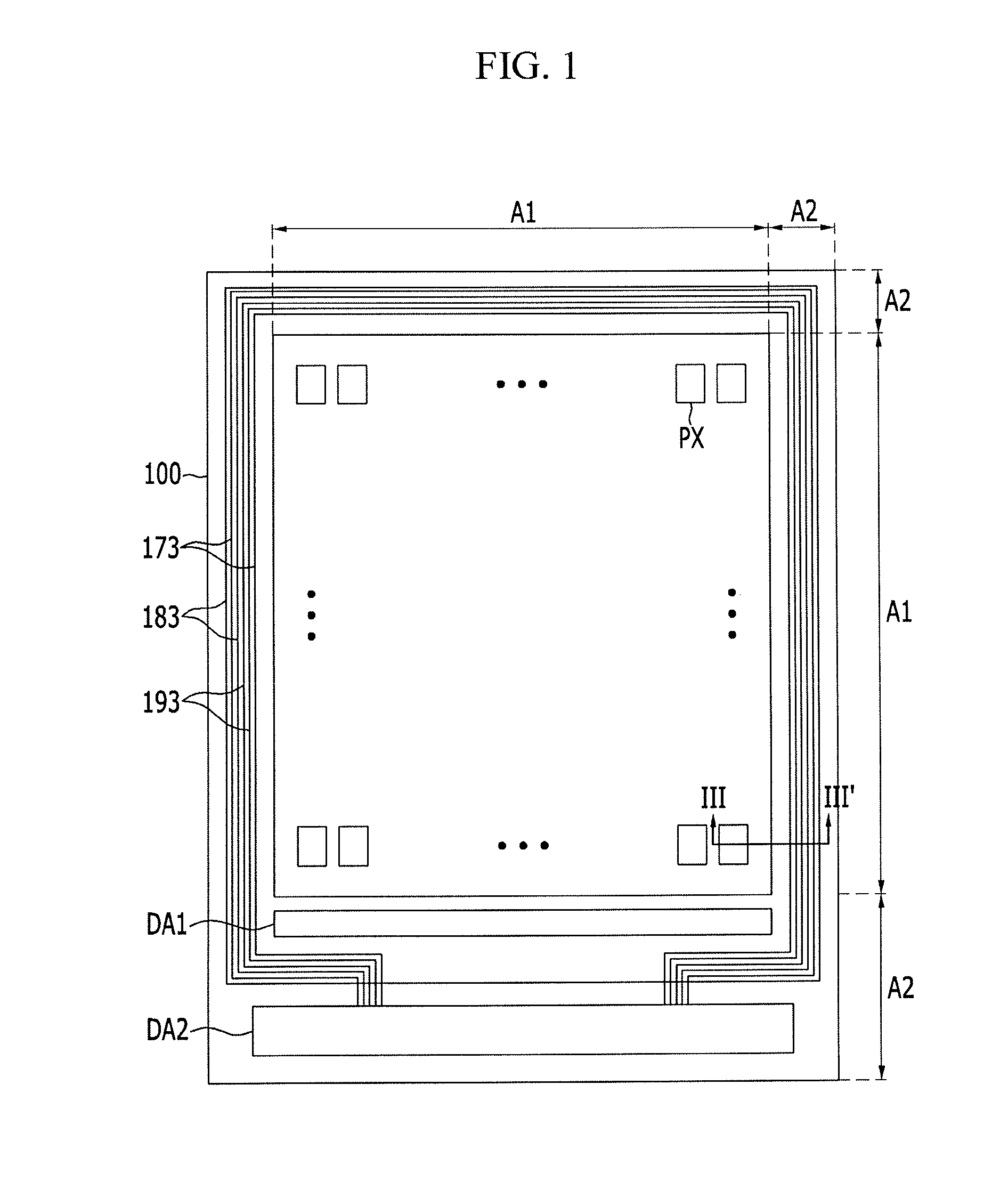
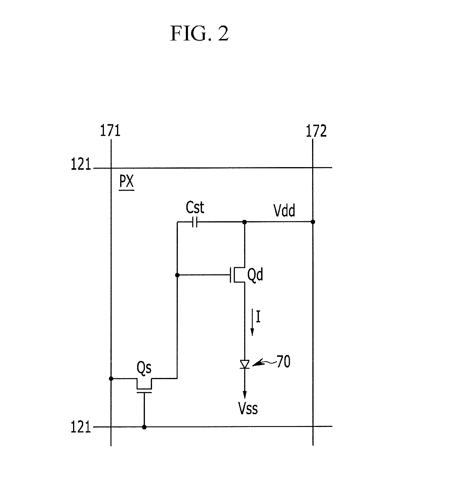
[0034]Exemplary embodiments of the present invention will be described more fully hereinafter with reference to the accompanying drawings. Like reference numerals may refer to like elements throughout the accompanying drawings.

[0035]In the drawings, the size and thickness of layers, films, panels, regions, etc., may be exaggerated for clarity. It will be understood that when an element such as a layer, film, region, or substrate is referred to as being “on”, “between”, “connected to”, “coupled to”, or “adjacent to” another element, it can be directly on, between, connected to, coupled to, or adjacent to the other element, or one or more intervening elements may also be present.

[0036]Spatially relative terms, such as “beneath”, “below”, “lower”, “under”, “above”, “upper” and the like, may be used herein for ease of description to describe one element or feature's relationship to another element(s) or feature(s) as illustrated in the figures. It will be understood that the spatially r...


PUM


Abstract

An organic light emitting diode (OLED) display includes a substrate including a pixel area and a surrounding peripheral area. The pixel area includes at least one pixel including an organic light emitting element. The OLED display includes a common voltage line disposed in the peripheral area and configured to transmit a common voltage to the pixel area, a barrier rib disposed on the substrate and covering one side of the common voltage line, a protection member covering another side of the common voltage line, at least one thin film transistor (TFT) disposed in the pixel area, a first electrode disposed in the pixel area and connected to the at least one TFT, an organic emission layer disposed on the first electrode, a second electrode disposed on the organic emission layer and connected to the common voltage line, and an encapsulation layer disposed on the protection member and the second electrode.

Description

CROSS-REFERENCE TO RELATED APPLICATIONS[0001]This application claims priority under 35 U.S.C. §119 to Korean Patent Application No. 10-2013-0094305 filed on Aug. 8, 2013, the disclosure of which is incorporated by reference herein in its entirety.TECHNICAL FIELD[0002]Exemplary embodiments of the present invention relate to an organic light emitting diode (OLED) display.DISCUSSION OF THE RELATED ART[0003]An organic light emitting diode (OLED) display includes two electrodes and an organic emission layer interposed therebetween. Electrons injected from a cathode that is one electrode, and holes injected from an anode that is another electrode, are bonded to each other in the organic emission layer to form excitons, and light is emitted while the excitons discharge energy.[0004]Each pixel of the organic light emitting diode display may include a switching thin film transistor, a driving thin film transistor, a capacitor, and an organic light emitting diode. A driving voltage is supplie...

Claims


Application Information

Patent Timeline
IPC IPC(8): H01L51/52H01L51/56H01L27/32H05B44/00
CPCH01L51/5253H01L51/56H01L27/3276H01L27/1248H10K59/122H10K59/1315H10K59/131H10K50/844H05B33/04H05B44/00H10K50/84H10K71/00H10K50/824
Inventor LEE, JAE-YONGKIM, YANG-WAN
Owner SAMSUNG DISPLAY CO LTD
Why Eureka
Try Eureka