
Semiconductor device

Active Publication Date: 2015-02-12
MARLIN SEMICON LTD
View PDF2 Cites 42 Cited by
  • Summary
  • Abstract
  • Description
  • Claims
  • Application Information

AI Technical Summary

Benefits of technology

The patent aims to create a semiconductor device with few defects and stronger stress on the channel region. This will enhance the efficiency and reliability of the device.

Problems solved by technology

However, along with the continuous decrease in the size and dimensions of the semiconductor devices, there are still some newly generated technological problems that need to be overcome, even though the non-planar transistor and the strained-silicon technology are already adopted.
For example, two adjacent epitaxial structures within the semiconductor device often generate unwanted lattice defects on their interfaces.
Therefore, how to effectively eliminate these defects and improve the performance of the semiconductor devices are important issues in this field.

Method used


Image

  • Semiconductor device
  • Semiconductor device
  • Semiconductor device

Examples


Embodiment Construction

[0014]In the following description, numerous specific details are given to provide a thorough understanding of the invention. It will, however, be apparent to one skilled in the art that the invention may be practiced without these specific details. Furthermore, some well-known system configurations and process steps are not disclosed in detail, as these should be well-known to those skilled in the art.

[0015]Likewise, the drawings showing embodiments of the apparatus are not to scale and some dimensions are exaggerated for clarity of presentation. Also, where multiple embodiments are disclosed and described as having some features in common, like or similar features will usually be described with same reference numerals for ease of illustration and description thereof(1656).

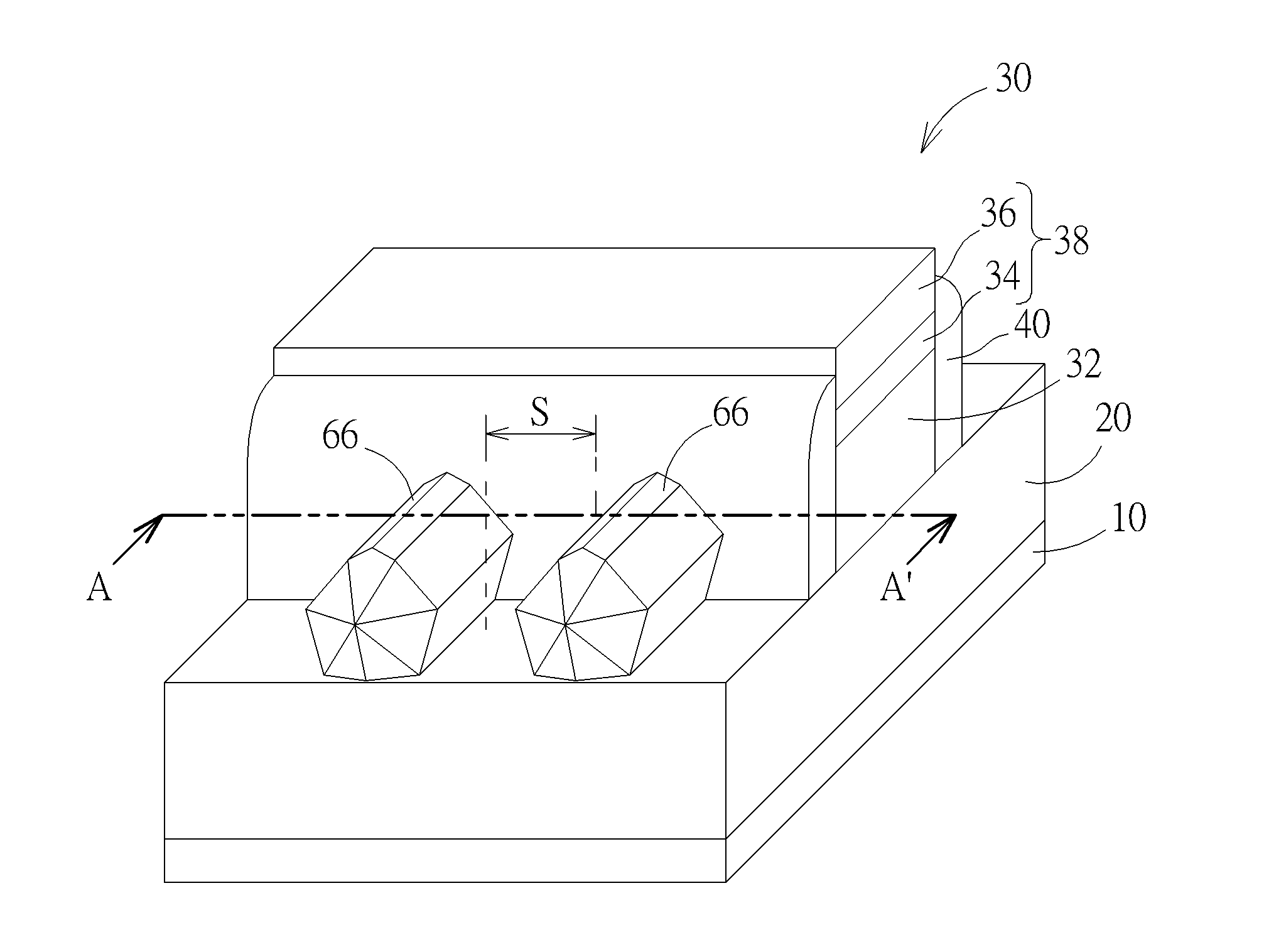
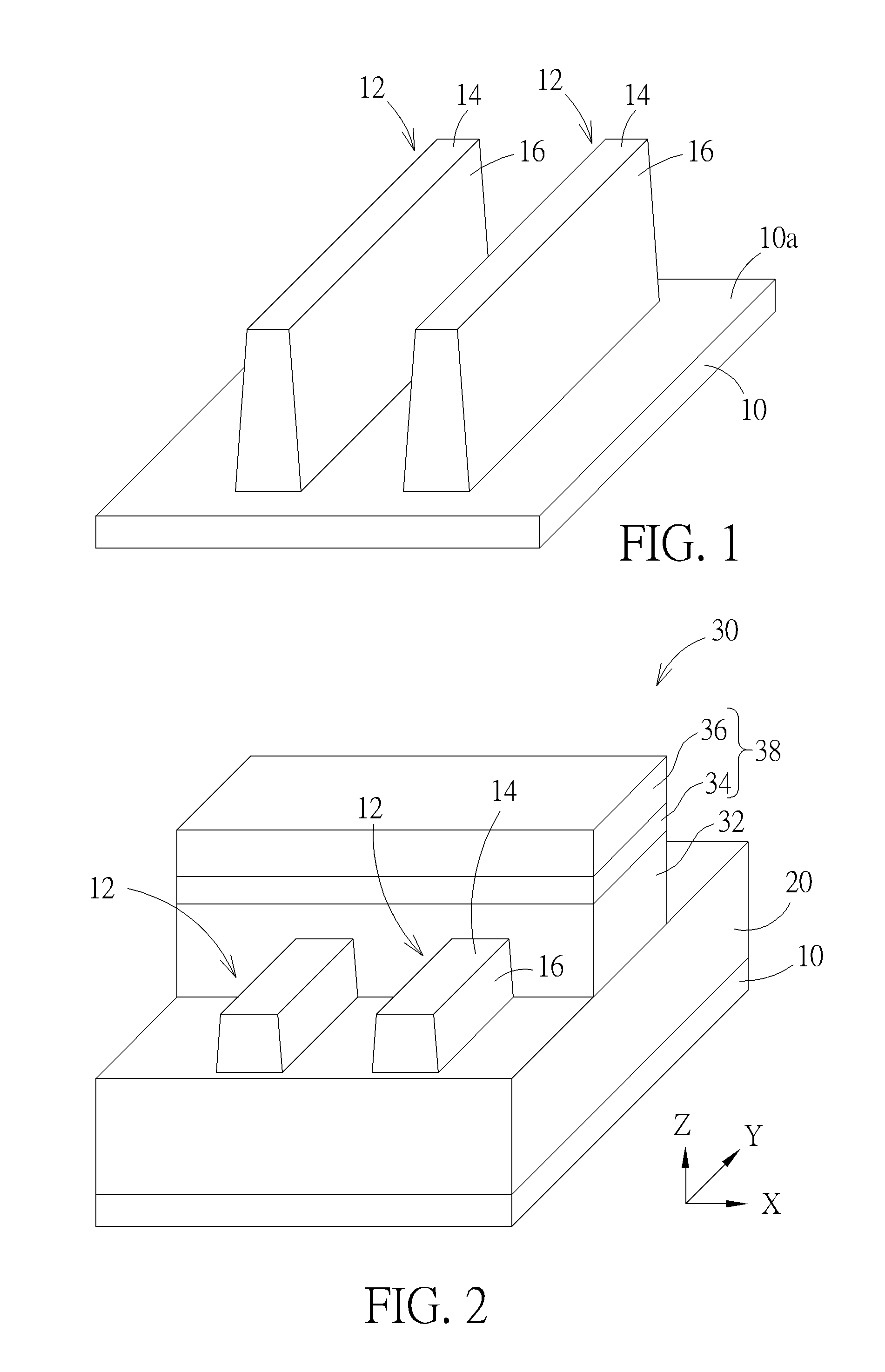
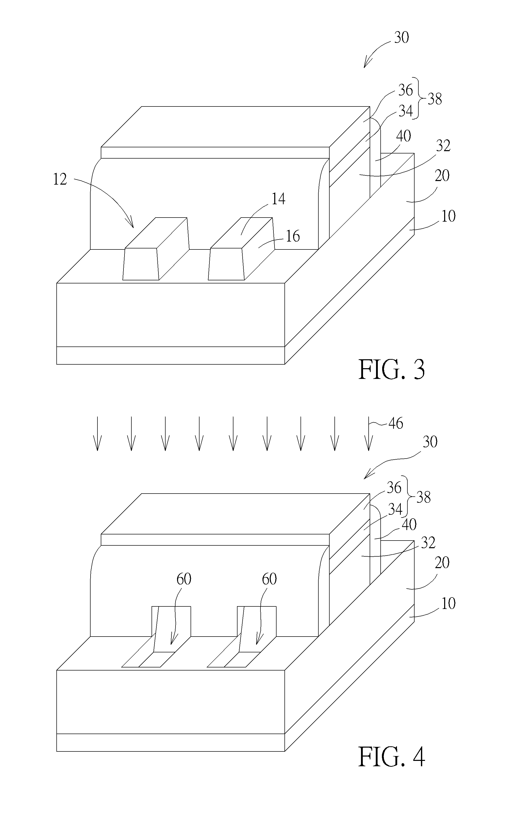
[0016]FIG. 1 to FIG. 8 are schematic diagrams showing a method for fabricating a semiconductor device according to a first preferred embodiment of the present invention. Please refer to FIG. 1. FIG. 1 is a schema...


PUM


Abstract

A semiconductor device includes at least two fin-shaped structures, a gate structure, at least two epitaxial structures and a silicon cap. The fin-shaped structures are disposed on a substrate and are covered by the gate structure. The epitaxial structures are disposed at one side of the gate structure and respectively directly contact each fin-shaped structure, wherein the epitaxial structures are spaced apart from each other. The silicon cap simultaneously surrounds the epitaxial structures.

Description

BACKGROUND OF THE INVENTION[0001]1. Field of the Invention[0002]The present invention generally relates to non-planar semiconductor devices, and more particular to non-planar semiconductor devices with epitaxial structures.[0003]2. Description of the Prior Art[0004]With the trend in the industry being towards scaling down the size of metal oxide semiconductor transistors (MOS), three-dimensional or non-planar transistor technology, such as the fin field effect transistor technology (Fin FET) has been developed to replace planar MOS transistors. The three-dimensional structure of a fin FET increases the overlapping area between the gate and the fin-shaped structure of the silicon substrate, and, accordingly, the channel region is more effectively controlled. The drain-induced barrier lowering (DIBL) effect and short channel effect (SCE) are therefore reduced. The channel region is also longer under the same gate length, and thus the current between the source and the drain is increas...

Claims


Application Information

Patent Timeline
IPC IPC(8): H01L29/417H01L29/78
CPCH01L29/7851H01L29/41791H01L29/66795H01L29/1608H01L29/165H01L29/7848H01L27/0886H01L29/161H01L29/267
Inventor LIAO, CHIN-ICHEN, CHUN-YU
Owner MARLIN SEMICON LTD
Learn More