Electroplating apparatus for tailored uniformity profile

a technology of uniformity and electroplating apparatus, which is applied in the direction of electrolysis process, semiconductor devices, electrolysis components, etc., can solve the problems of current crowding, increased plating at certain azimuthal regions of the wafer, and unwanted ionic current crowding, so as to maximize the randomization of flow patterns

Active Publication Date: 2015-03-05
NOVELLUS SYSTEMS
View PDF3 Cites 12 Cited by
  • Summary
  • Abstract
  • Description
  • Claims
  • Application Information

AI Technical Summary

Benefits of technology

The techniques described in this patent include a method to optimize the flow of electrolyte during electroplating for the fabrication of semiconductor devices. This is achieved by rotating a protective shield with a removed segment that is placed close to the wafer surface. This will cause the electrolyte to flow laterally at the wafer surface in the direction of the shield's opening, resulting in a more even distribution of electrolyte around the wafer. By rotating the shield at a different speed from the wafer, the flow patterns are maximized, which improves the overall quality and efficiency of the semiconductor device fabrication process.

Problems solved by technology

The asymmetry refers not only to purely geometric asymmetry of the substrate (such as presence of a notch, or a flat region cut along a chord), but also to asymmetry within the features on the substrate, which may result in unwanted ionic current crowding during plating, and lead to increased plating at certain azimuthal regions of the wafer.
Electroplating on such substrate leads to current crowding in the areas that are adjacent to the azimuthal variable patterning discontinuities at the periphery, such as a region with missing features and missing die, and, consequently, to plating non-uniformity in this region.

Method used


Image

  • Electroplating apparatus for tailored uniformity profile
  • Electroplating apparatus for tailored uniformity profile
  • Electroplating apparatus for tailored uniformity profile

Examples


Embodiment Construction

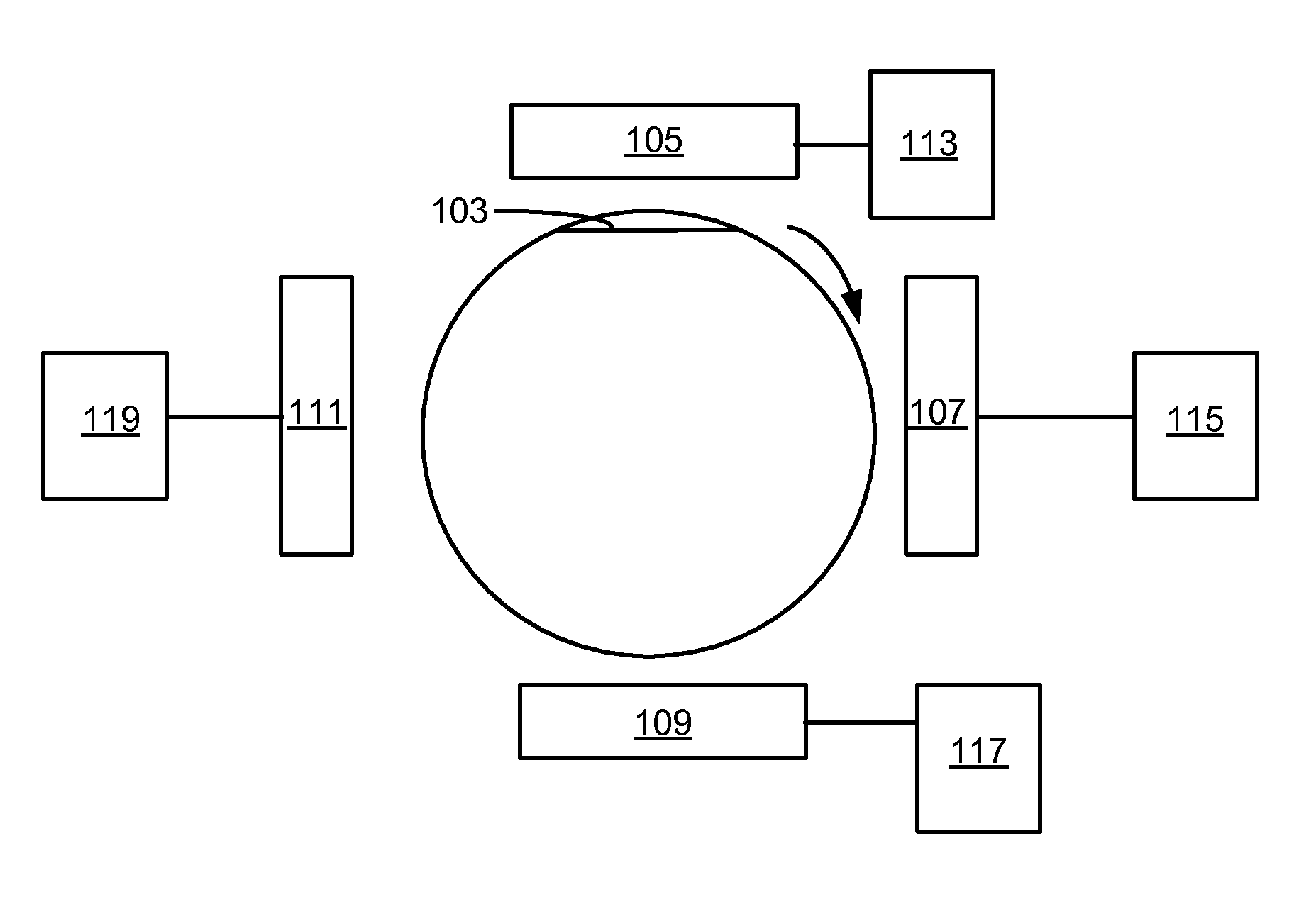
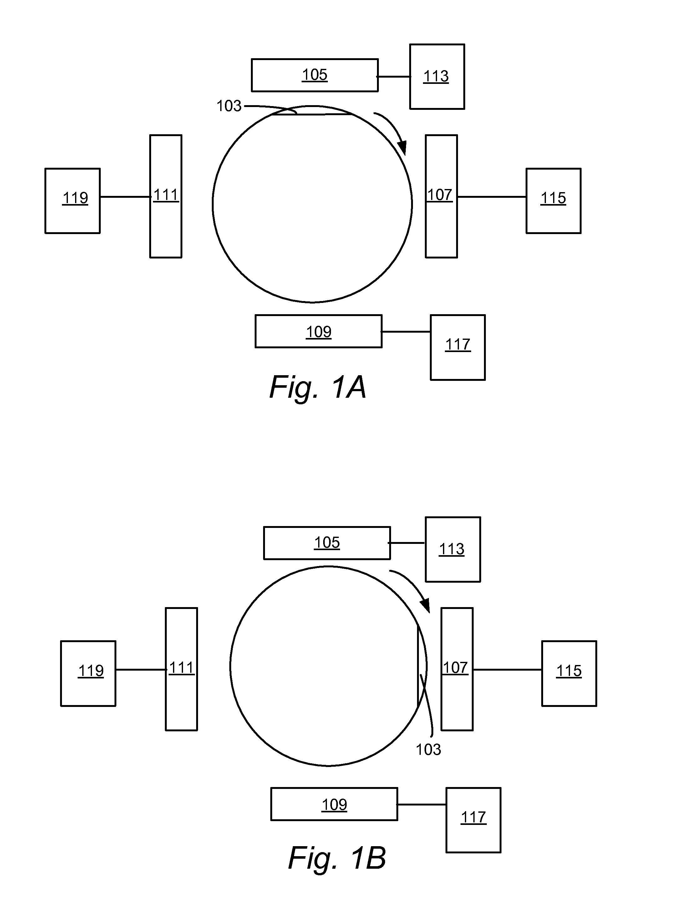
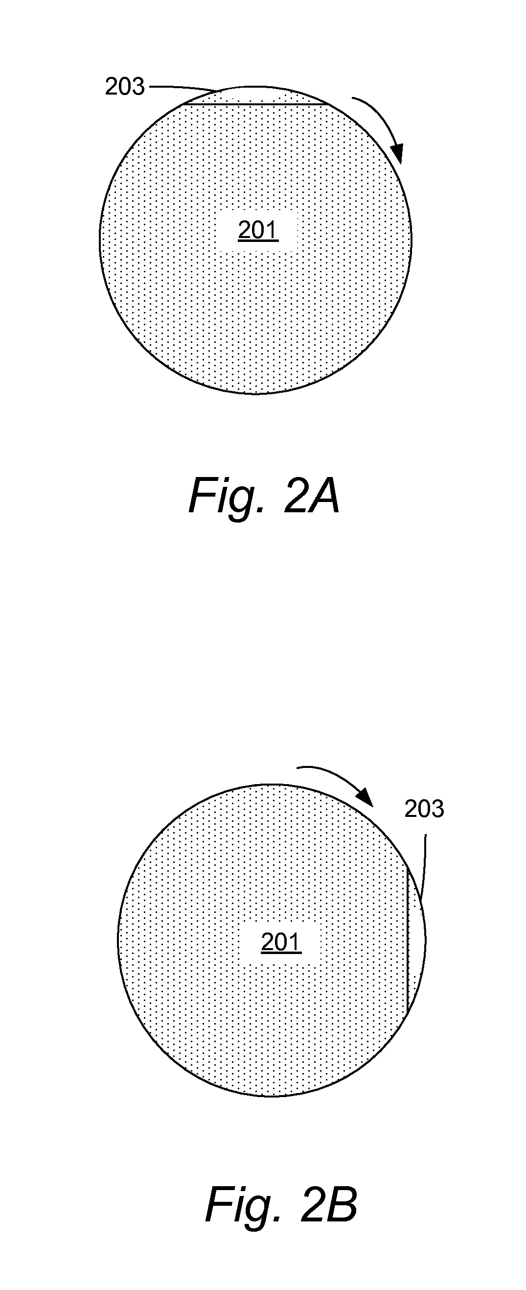
[0065]Methods and apparatus for electroplating a metal on a substrate while controlling uniformity of the electroplated layer, such as azimuthal uniformity, radial uniformity, or both, are provided.

[0066]Embodiments are described generally where the substrate is a semiconductor wafer; however the invention is not so limited. Provided apparatus and methods are useful for electroplating metals in TSV and WLP applications, but can also be used in a variety of other electroplating processes, including deposition of copper in damascene features. Examples of metals that can be electroplated using provided methods include, without limitation, copper, tin, a tin-lead composition, a tin-silver composition, nickel, cobalt, nickel and / or cobalt alloys with each other and with tungsten, a tin-copper composition, a tin-silver-copper composition, gold, palladium, and various alloys which include these metals and compositions.

[0067]In a typical electroplating process, the semiconductor wafer subst...


PUM

PropertyMeasurementUnit
voltageaaaaaaaaaa
diameteraaaaaaaaaa
diameteraaaaaaaaaa

Abstract

Methods of electroplating metal on a substrate while controlling azimuthal uniformity, include, in one aspect, providing the substrate to the electroplating apparatus configured for rotating the substrate during electroplating, and electroplating the metal on the substrate while rotating the substrate relative to a shield such that a selected portion of the substrate at a selected azimuthal position dwells in a shielded area for a different amount of time than a second portion of the substrate having the same average arc length and the same average radial position and residing at a different angular (azimuthal) position. For example, a semiconductor wafer substrate can be rotated during electroplating slower or faster, when the selected portion of the substrate passes through the shielded area.

Description

CROSS-REFERENCE TO RELATED APPLICATIONS[0001]This application is a continuation claiming priority to U.S. patent application Ser. No. 13 / 438,443, titled “Electroplating Apparatus for Tailored Uniformity Profile” naming Mayer et al. as inventors, filed Apr. 3, 2012, which claims benefit under 35 U.S.C. §119(e) to U.S. Provisional Patent Application No. 61 / 471,624, titled “Electroplating Apparatus for Tailored Uniformity Profile”, naming Mayer et al. as inventors, filed Apr. 4, 2011 and to U.S. Provisional Patent Application No. 61 / 598,054, titled “Electroplating Apparatus for Uniform Electrolyte Flow Distribution” naming Buckalew et al. as inventors, filed Feb. 13, 2012, which are herein incorporated by reference. U.S. patent application Ser. No. 13 / 438,443 is also a continuation-in-part claiming priority to U.S. patent application Ser. No. 12 / 291,356, titled “Method and Apparatus for Electroplating” naming Reid et al. as inventors, filed Nov. 7, 2008, now U.S. Pat. No. 8,308,931, is...

Claims


Application Information

Patent Timeline
Patent Type & Authority Applications(United States)
IPC IPC(8): C25D21/12C25D5/04
CPCC25D5/04C25D21/12C25D5/18C25D17/001C25D17/007C25D17/008C25D17/12C25D21/10H01L21/2885H01L21/76873C25D5/028C25D7/123C25D17/002C25D17/06
Inventor MAYER, STEVEN T.PORTER, DAVID W.BUCKALEW, BRYAN L.RASH, ROBERT
Owner NOVELLUS SYSTEMS
Why Eureka
Try Eureka