Split Gate Nanocrystal Memory Integration

a technology of nanocrystals and nanocrystals, applied in the field of integrated circuit devices, can solve problems such as feature sizes

Active Publication Date: 2015-03-05
NXP USA INC
View PDF19 Cites 43 Cited by
  • Summary
  • Abstract
  • Description
  • Claims
  • Application Information

AI Technical Summary

Problems solved by technology

While the introduction of novel gate stack materials for forming high-k metal gate stacks using gate last processes has improved device performance and reduced feature sizes for transistor

Method used


Image

  • Split Gate Nanocrystal Memory Integration
  • Split Gate Nanocrystal Memory Integration
  • Split Gate Nanocrystal Memory Integration

Examples


Embodiment Construction

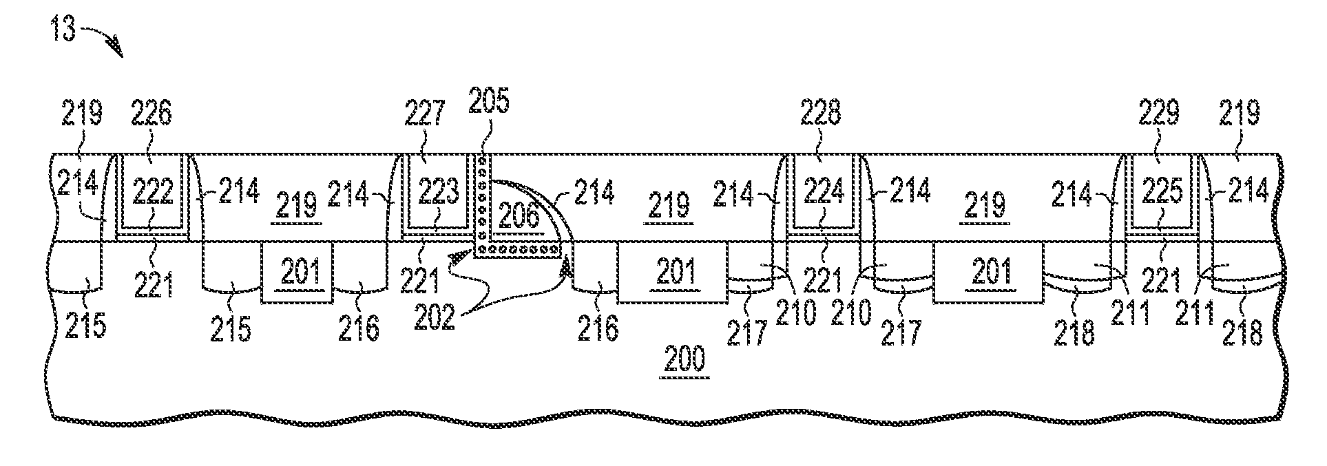
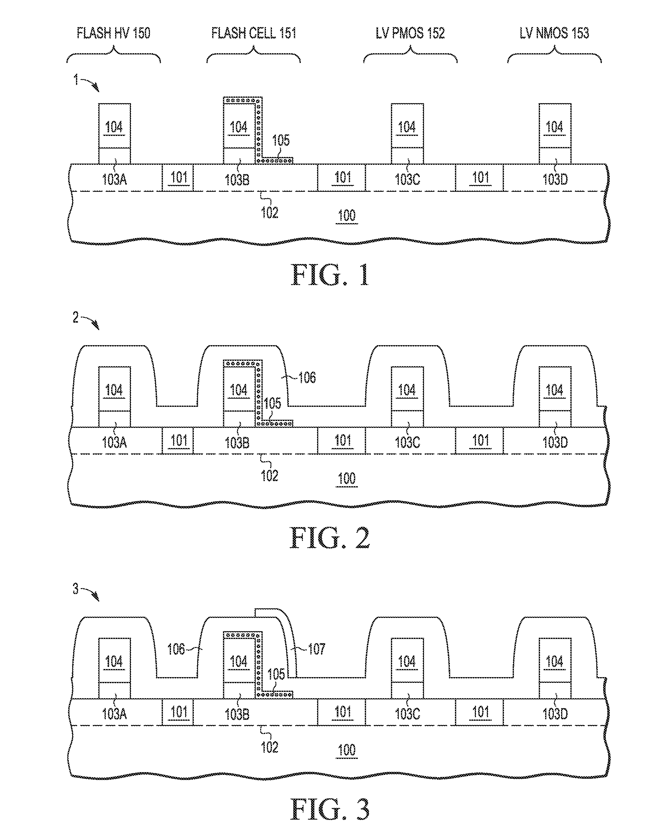
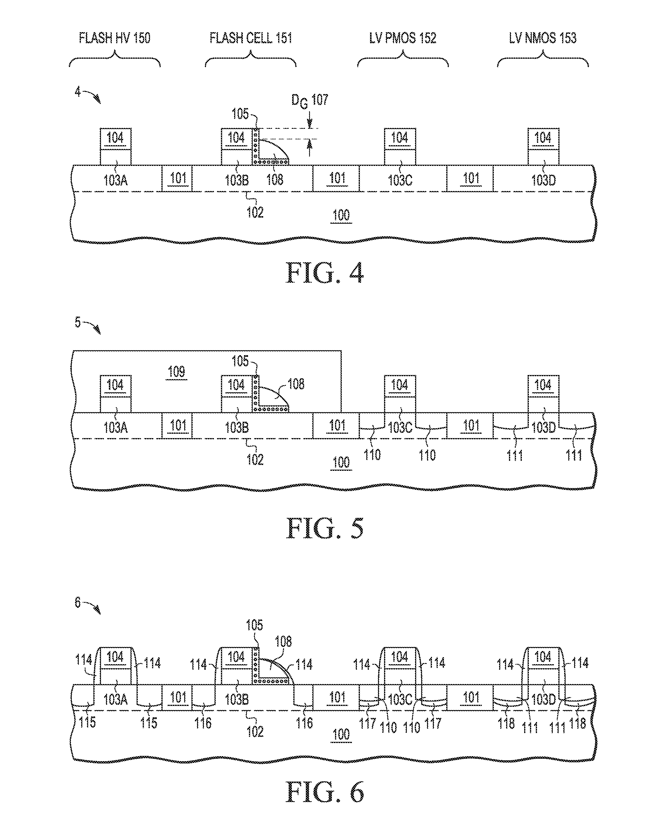
[0010]A compact split-gate nanocrystal thin film storage (TFS) non-volatile memory (NVM) bitcell integrated with high-k metal gate (HKMG) transistors and associated fabrication process are disclosed in which the NVM bitcells are formed with a spacer control gate and an HKMG select gate that is formed along with non-NVM HKMG transistor gates using a CMOS gate-last fabrication sequence to enable the co-existence of embedded flash and HKMG transistors on the same wafer. In selected embodiments, the spacer control gates are formed on recessed substrate control gate channel regions to lower the top of the spacer control gate relative to the top of sacrificial select gates used to form the HKMG select gate. After patterning a poly layer with a first gate pattern to define one or more sacrificial poly select gates over an NVM area and one or more sacrificial poly transistor gates in the non-NVM area, a nanocrystal stack (or other charge storage layer) and spacer control gate are formed nex...


PUM


Abstract

A process integration is disclosed for fabricating non-volatile memory (NVM) cells having spacer control gates (108) along with a high-k-metal-poly select gate (121, 123, 127) and one or more additional in-laid high-k metal CMOS transistor gates (121, 124, 128) using a gate-last HKMG CMOS process flow without interfering with the operation or reliability of the NVM cells.

Description

BACKGROUND OF THE INVENTION[0001]1. Field of the Invention[0002]The present invention is directed in general to integrated circuit devices and methods for manufacturing same. In one aspect, the present invention relates to the fabrication of CMOS metal gate devices and non-volatile memory devices integrated on a single substrate or chip.[0003]2. Description of the Related Art[0004]Non-volatile memory devices, such as EEPROM and flash memory, are used in computers and other electronic devices to store data and / or programming instructions that can be electrically erased and reprogrammed and that must be saved when power is removed. Embedded non-volatile memory (NVM) has become increasingly important in applications ranging from data and code storage to circuit trimming and customization. By embedding a non-volatile memory in a CMOS device, a single chip device can be manufactured and configured for a variety of applications. While the introduction of novel gate stack materials for for...

Claims


Application Information

Patent Timeline
IPC IPC(8): H01L27/115H01L29/49H01L21/28
CPCH01L27/11563H01L29/49H01L21/28008H01L29/42332H01L29/66825H01L29/517H01L29/66545H01L29/6659H01L29/40117H01L29/40114H10B41/49H01L29/42344
Inventor LOIKO, KONSTANTIN V.WINSTEAD, BRIAN A.
Owner NXP USA INC
Why Eureka
Try Eureka