Dense-pitch small-pad copper wire bonded double IC chip stack packaging piece and preparation method therefor

Active Publication Date: 2015-03-05
TIANSHUI HUATIAN TECH +1
View PDF0 Cites 5 Cited by
  • Summary
  • Abstract
  • Description
  • Claims
  • Application Information

AI Technical Summary

Benefits of technology

[0033]A multiple-ball welding method is adopted for the package of the present invention. To be specific, a metal ball is firstly implanted on an IC chip pad; moreover, a copper bonding ball is welded on the metal ball and a structure of the copper bonding ball is directly welded on rest pads, thus avoiding the crater on the pad and a short circuit of adjacent welding spots, which not only solves the problem of an open circuit of a plastic packaging punching wire caused by ease damage of a previous wire during dense-pitch small-pad high density bonding, but also avoids the difficulty of a short circuit of adjacent welding

Problems solved by technology

The size change of the pad brings difficulty and great challenge for the bonding process.
Actually, the distance between the two adjacent bonding wires cannot meet general quality requirements even if the wire diameter is removed and the clearance between the adjacent bonding wires is 1.69˜1.86 times of the wire diameter.
However, for dense-pitch small-pad bonding, it is very difficult to control the diameter of a bonding wall.
A little carelessness may make the bonding ball exceed

Method used


Image

  • Dense-pitch small-pad copper wire bonded double IC chip stack packaging piece and preparation method therefor
  • Dense-pitch small-pad copper wire bonded double IC chip stack packaging piece and preparation method therefor
  • Dense-pitch small-pad copper wire bonded double IC chip stack packaging piece and preparation method therefor

Examples


embodiment 1

[0044]1. Load the chip

[0045]1) Thin and scribe

[0046]Adopt related packaging form thinning standard equipment and process to thin a wafer to 210 μm through a conventional method and scribe.

[0047]2) Load the chip for the first time

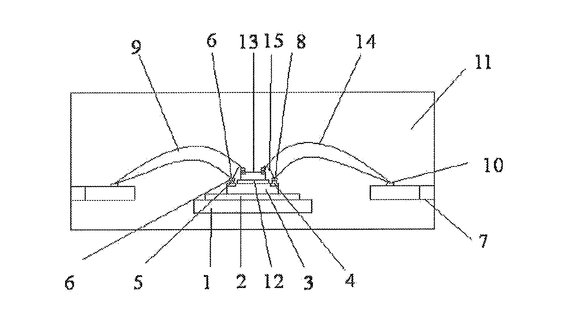
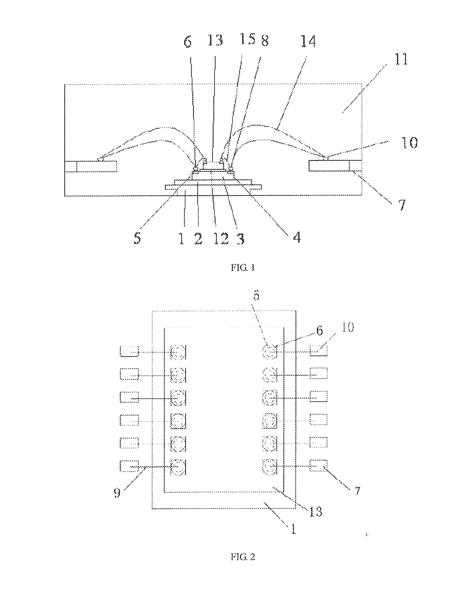
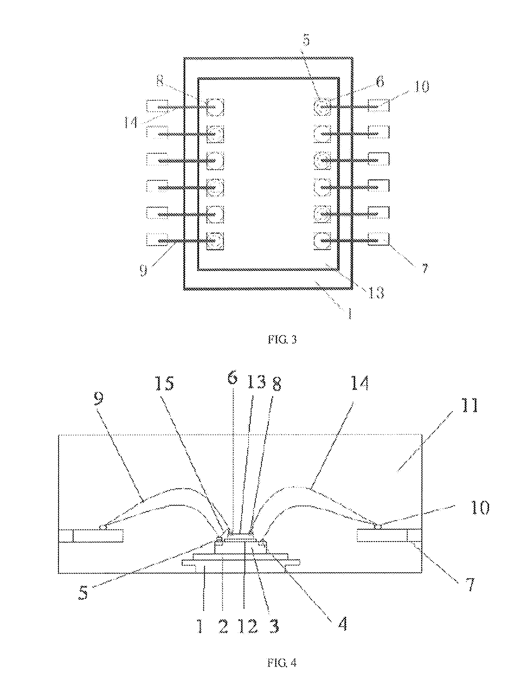
[0048]Adopt eSOP, eMSOP, eTSSOP, eL / TQFP, QFN and DFN lead frame with a carrier exposed to fix the thinned and scribed first IC chip 3 to 210 μm on the lead frame carrier 1 through a chip adhesive 2, and collect the first IC chips 3 into a transfer box after all the first IC chips are adhered in sequence.

[0049]3) Load the chip for the second time

[0050]Feed the transfer box in which all the first IC chips 3 are adhered to the feeding position of a loading machine which ascends to a set position automatically. Transfer one chip to the center of a machine table. Fix the chip through an orbit pressing plate. Dispense an insulating adhesive 12 on the first IC chip 3. An automatic suction nozzle of the loading machine automatically absorb and place the first IC ch...

embodiment 2

[0064]1. Load the chip

[0065]1) Thin and scribe

[0066]Adopt related packaging form thinning standard equipment and process to thin a lower wafer to 210 μm and an upper wafer to 150 μm through a conventional method and scribe.

[0067]2) Load the chip for the first time

[0068]Adopt eSOP, eMSOP, eTSSOP, eL / TQFP, QFN and DFN lead frame with a carrier exposed to fix the thinned and scribed first IC chip 3 to 210 μm on the lead frame carrier 1 through a conductive adhesive 2 and collect the first IC chips 3 into a transfer box after all the first IC chips are adhered in sequence.

[0069]3) Load the chip for the second time

[0070]Feed the transfer box in which all the first IC chips 3 are adhered to the feeding position of a loading machine which ascends to a set position automatically. Transfer one chip to the center of a machine table. Fix the chip through an orbit pressing plate. Dispense an insulating adhesive 12 on the first IC chip 3. An automatic suction nozzle of the loading machine automa...

embodiment 3

[0084]1. Load the chip

[0085]1) Thin and scribe

[0086]Adopt related packaging form thinning standard equipment and process to thin a wafer to 210 μm through a conventional method and scribe.

[0087]2) Load the chip for the first time

[0088]Adopt SOP, MSOP, SSOP, TSSOP, QFP, L / TQFP, QFN, DFN lead frame with a carrier not exposed to fix the thinned and scribed first IC chip 3 to 210 μm on the lead frame carrier 1 through an insulating adhesive 2 and collect the first IC chips 3 into a transfer box after all the first IC chips are adhered in sequence.

[0089]3) Load the chip for the second time

[0090]Feed the transfer box in which all the first IC chips 3 are adhered to the feeding position of a loading machine which ascends to a set position automatically. Transfer one chip to the center of a machine table. Fix the chip through an orbit pressing plate. Dispense an insulating adhesive 12 on the first IC chip 3. An automatic suction nozzle of the loading machine automatically absorb and place t...


PUM


Abstract

A dense-pitch small-pad copper wire bonded double IC chip stack package comprises a plastic package body, in which a lead frame carrier and a frame lead inner pin are arranged; the upper surface of the lead frame carrier is fixedly connected with a first IC chip; a second IC chip is stacked on the first IC chip; the upper surface of the first IC chip and the upper surface of the second IC chip are respectively provided with a plurality of pads which are arranged as two lines of pad groups in parallel; the two pad groups are respectively a first pad group and a second pad group; a metal ball is implanted on each pad; each metal ball is connected with a first copper bonding ball; and a third copper bonding wire is formed by looping and arching on a corresponding metal ball between the second IC chip and the first IC chip. The preparation process of the present invention comprises thinning, scribing, loading the chip, performing pressure welding, plastic packaging and post-curing, trimming, electroplating, printing, forming and separating, and packaging. The package and the preparation method of the invention avoid the hidden danger of open circuit of a plastic packaging punching wire caused by the crater on the pad, the short circuit of adjacent welding spots, and the easy damage of a previous wire.

Description

FIELD OF THE INVENTION[0001]The present invention belongs to the field of electronic information automation component and part manufacturing technology, and relates to an IC chip package, and in particular, to a dense-pitch small-pad copper wire bonded double IC chip stack package. The present invention further relates to a preparation method of the package.BACKGROUND OF THE INVENTION[0002]With the rapid development of the electronic information industry, a chip manufacturing industry moves into a nanometer times. A chip manufacturing process size is reduced from 90 nm to 45 nm, and then to 30 nm and 13 nm, which is quickly progressed. The physical dimension of the chip is more and more small, which is from 1.0 μmm×1.0 μmm to 0.8 μmm×0.8 μmm, 0.5 μmm×0.5 μmm, 0.3 μmm×0.3 μmm, and minimum 0.15 μmm×0.15 μmm. Accordingly, the pitch of the pad used for chip manufacturing is gradually reduced from 120 μm to 100 μm, 70 μm, 60 μm, 50 μm and 45 μm. and a scribing channel is also gradually r...

Claims


Application Information

Patent Timeline
IPC IPC(8): H01L25/065H01L23/495H01L25/00
CPCH01L25/0657H01L25/50H01L2225/0651H01L23/4952H01L2225/06506H01L23/49575H01L2224/32145H01L2224/32245H01L2224/48145H01L2224/48247H01L2224/73265H01L2224/45147H01L23/3107H01L24/05H01L24/06H01L24/32H01L24/45H01L24/48H01L24/49H01L24/73H01L24/75H01L24/85H01L24/97H01L2224/04042H01L2224/05554H01L2224/06135H01L2224/48464H01L2224/49109H01L2224/49175H01L2224/75745H01L2224/92247H01L2224/97H01L2224/75704H01L2224/45015H01L2224/85H01L2924/181H01L2224/4848H01L2224/48091H01L2924/14H01L2224/49427H01L2924/10161H01L2924/00012H01L2224/83H01L2924/00H01L2924/00014H01L2924/20751H01L2924/00015H01L2224/48147
Inventor MU, WEILI, XIZHOUGUO, XIAOWEI
Owner TIANSHUI HUATIAN TECH
Why Eureka
Try Eureka