Eureka AIR delivers breakthrough ideas for toughest innovation challenges, trusted by R&D personnel around the world.

Method for power estimation for virtual prototyping models for semiconductors

Active Publication Date: 2015-03-05
HUILGOL NINAD
View PDF1 Cites 9 Cited by
  • Summary
  • Abstract
  • Description
  • Claims
  • Application Information

AI Technical Summary

Benefits of technology

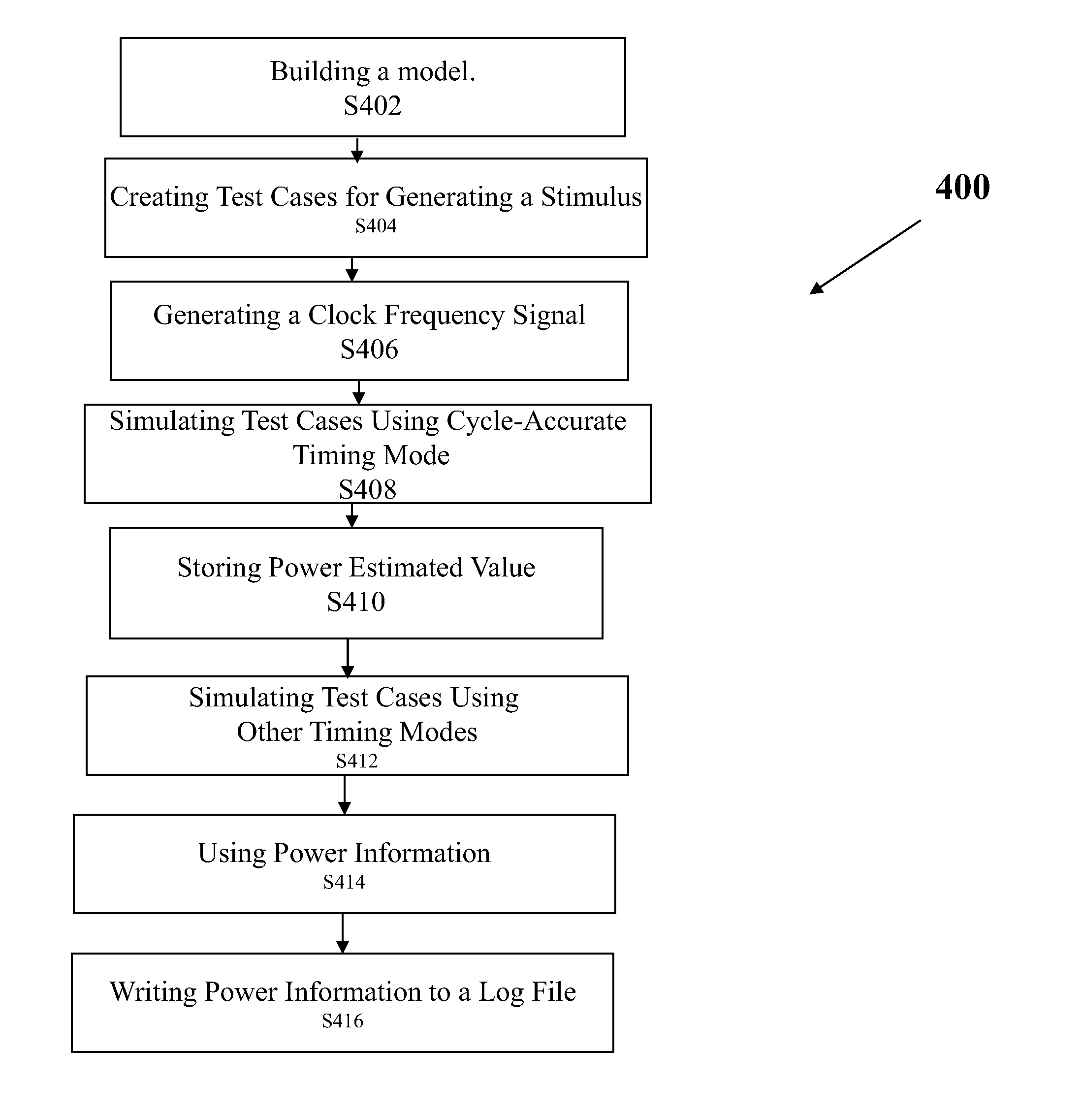
The present invention provides a method for measuring power in a virtual prototype of a model semiconductor design, which involves identifying transistors in a netlist and generating a measurement statement for each transistor usable by a circuit simulation tool to measure power consumption without synthesizing the model. A measurement file is created and placed in a circuit simulation tool for performing the simulation of the integrated circuit. The invention also provides a method for power evaluation for multiple modules of an electronic system, which involves analyzing a circuit description, identifying equivalent operations, and generating power macro-models for each operation of module using those previously analyzed cases and the context of input stimuli under which the circuit is exercised. A monitor file is produced wherein the testbench description is associated with a pair of print statements for each segment in the test bench description. The technical effects of the invention include improved accuracy and efficiency in evaluating power consumption of a semiconductor design during simulation.

Problems solved by technology

Because of limited battery life, reliability issues, and packaging and cooling costs, power consmption for devices is a critical design concern.
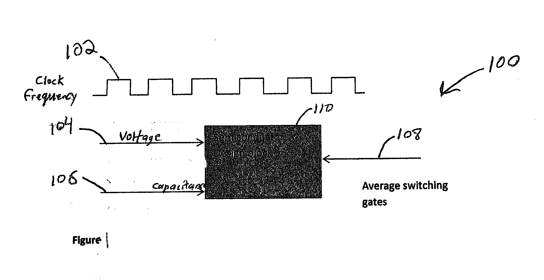
Since the real clock signal cycles many times during simulations, the simulations tend to be very slow, as each clock cycle (or “tick”) necessitates evaluation of the simulator events.
Thus, simulating real world conditions which happen over several minutes becomes extremely slow.
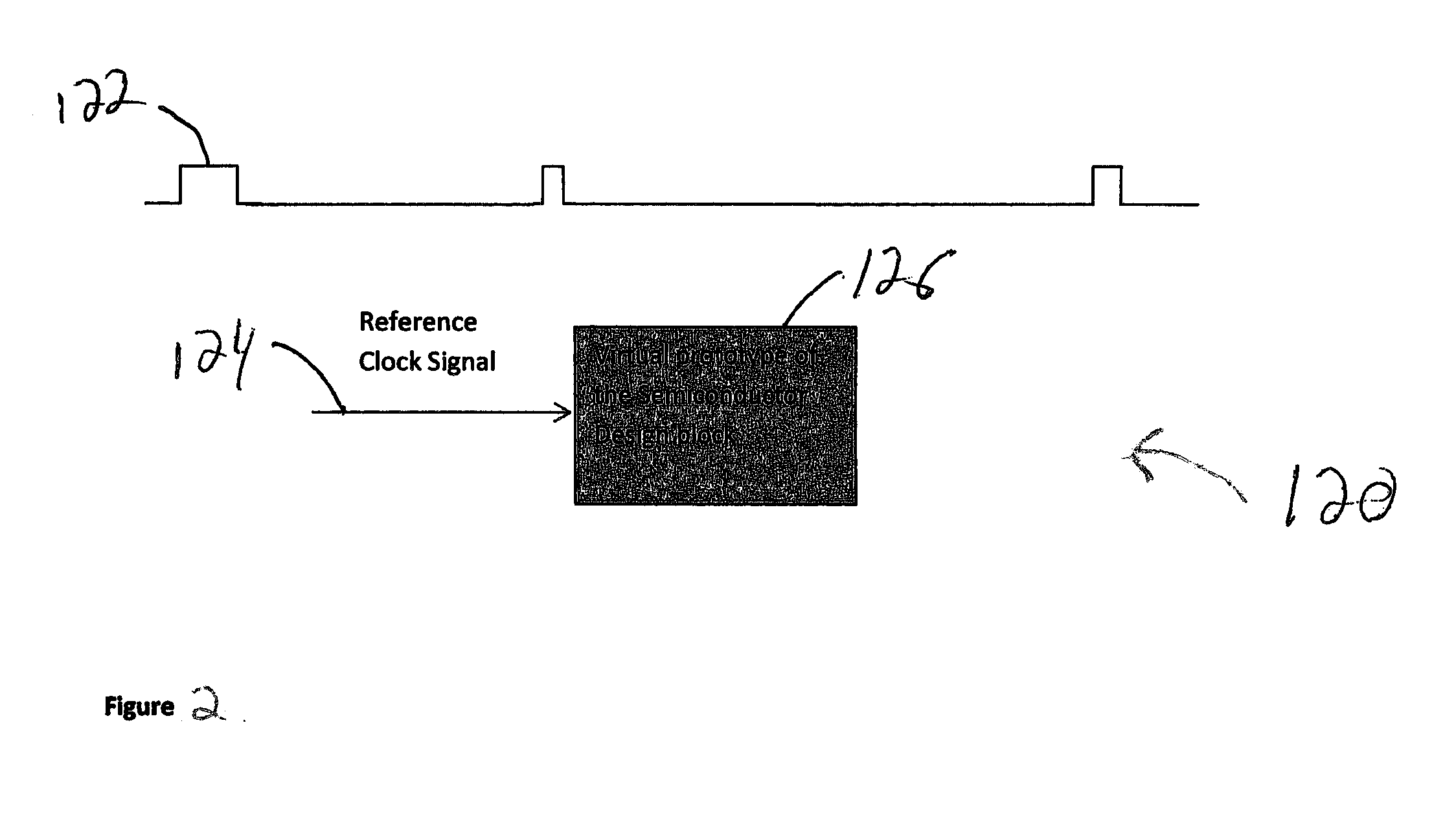
There is no “cycle accurate” mode prescribed by Accelera when building and simulating a virtual prototype.
However, in a virtual prototype of the semiconductor design, any power estimation will not be accurate.
Power estimation can be hampered in complexity, time, and cost, by engaging in model synthesis.
Power estimation without performing the model synthesis step, has been avoided due to the industry's failure to develop a method of estimating power that excludes model synthesis.

Method used


Image

  • Method for power estimation for virtual prototyping models for semiconductors
  • Method for power estimation for virtual prototyping models for semiconductors
  • Method for power estimation for virtual prototyping models for semiconductors

Examples


Embodiment Construction

[0025]The following detailed description is of the best currently contemplated modes of carrying out the invention. The description is not to be taken in a limiting sense, but is made merely for the purpose of illustrating the general principles of the invention, since the scope of the invention is best defined by the appended claims.

[0026]Model synthesis, such as logic synthesis, entails costs, time expenditure, and manpower. For power estimation using model synthesis of virtual prototypes, wherein architectural exploration and system level performance analysis are important goals, power estimation may be achieved without full model synthesis, saving excessive costs, time, and manpower. This invention provides a method to estimate power in a virtual prototype without model synthesis.

[0027]A virtual prototype of a semiconductor design consists of many blocks, each performing a specific task. Each block can have either a single clock, or multiple clocks supplied to it. Every block mi...


PUM


Abstract

The present invention may comprise an apparatus and method for calculating power consumption, including a unit for generating a clock-level analysis without synthesis of an algorithm description and calculating operating ratios of storage elements and arithmetic units. The invention may also comprise a method for estimating the power to be consumed by a SystemC model. By estimating this value, a user may gauge the amount of power a specific semiconductor design might consume, once manufactured into a chip.

Description

CROSS-REFERENCE TO RELATED APPLICATION[0001]The application claims priority from U.S. Provisional Patent Application No. 61 / 696,213, filed Sep. 2, 2012, the contents of which are incorporated herein by reference.BACKGROUND OF THE INVENTION[0002]The present invention relates generally to virtual prototyping. Specifically, the invention relates to a method for predictive simulation and power estimation of microdevices and microsystems.[0003]Portable and high-density micro-electronic devices make power dissipation of very large scale integrated (VLSI) circuits a critical concern. Because of limited battery life, reliability issues, and packaging and cooling costs, power consmption for devices is a critical design concern. To avoid issues associated with excessive power consumption, computer design helps to estimate power consumption of VLSI designs.[0004]The rapid progress in microsystems technology is increasingly supported by specific modeling methods and dedicated simulation tools. ...

Claims


Application Information

Patent Timeline
IPC IPC(8): G06F17/50
CPCG06F17/5045G06F2119/06G06F30/367G06F30/398G06F30/20
Inventor HUILGOL, NINAD
Owner HUILGOL NINAD
Why Eureka
Eureka Blog
Learn More