Vcsel module and manufacture thereof

a technology of vcsel modules and modules, which is applied in the direction of lasers, semiconductor laser arrangements, semiconductor lasers, etc., can solve the problems of inflexibility, increased production costs, and increased production costs of vcsel modules, so as to reduce outcoupling losses and facilitate connection

Active Publication Date: 2015-03-12
TRUMPF PHOTONIC COMPONENTS GMBH
View PDF4 Cites 19 Cited by
  • Summary
  • Abstract
  • Description
  • Claims
  • Application Information

AI Technical Summary

Benefits of technology

[0016]By this measure, the overall current necessary to run all the VCSEL units of one VCSEL chip can be substantially reduced, namely by a factor which is essentially equal to the number of subarrays in series. Thus, the maximum operation current Imax of a chip (for instance 40 A for a chip of the size of 3×3 mm) can be reduced to Imax / n, with n being the number of subarrays in series. Compared to the previous technique of mounting n smaller chips in series on a submount with, for instance, n=4, a reduction of 75% of all solder steps can be achieved. Further, placement steps can be simplified and wire-bonding can be virtually eliminated To conclude, this measure makes it possible to mount a lot more VCSEL units on one chip without going over the limits of the overall VCSEL system, in particular the driver and the electrical connections. The size of VCSEL chips can be increased substantially, which makes the mounting process more convenient and even safer: Larger VCSEL chips means that less chips need to be mounted to achieve the same laser performance and thus less work and less solder connections are necessary. In addition, the necessary wafer area of the VCSEL chip is smaller due to a reduction of sawing lanes, as is the overall area of the entire VCSEL module as there are less air gaps between individual VCSEL chips.
[0048]The carrier material is preferably added to the rest of the semi-finished VCSEL product by a bonding, and / or filling process. A bonding process may for instance comprise a glueing process. Apart from glueing, other techniques such as direct bonding, (laser-selective) soldering, laser-assisted bonding, may be used. Use is thus made of a bonding, e.g. glueing and / or filling material which for instance fills lower regions, i.e. gaps, between the mesas of the VCSEL units so that the carrier material can be evenly applied to the semi-finished VCSEL product. At the same time, this material functions as a bonding means which connects the carrier material to the rest of the semi-finished VCSEL product. Thereby, it is preferred that the bonding and / or filling material used in the bonding and / or filling process has after curing essentially the same refractive index as the carrier material. This way it is made sure that no optical disturbances occur due to the bonding / filling material.

Problems solved by technology

The larger these chips the less mounting time and thus mounting costs for the production of VCSEL modules needs to be spent.
Firstly, larger chips reduce the amount of lost wafer area due to sawing lanes and rims of the chips.
The sizes of VCSEL chips are mainly limited by the current that runs through them.
In addition, the size of the electrical connections from such driver to the VCSEL module and inside of the VCSEL module scale up with the operation current and become more and more bulky, heavy, and inflexible.
For larger chips however, the current is the limiting factor of size, because on the chip level all VCSEL units are operated in parallel.
This implies that there is a certain limit of size to VCSEL chips inside VCSEL modules which limit also restricts the effectivity of mounting processes of the VCSEL chips.

Method used


Image

  • Vcsel module and manufacture thereof
  • Vcsel module and manufacture thereof
  • Vcsel module and manufacture thereof

Examples


Embodiment Construction

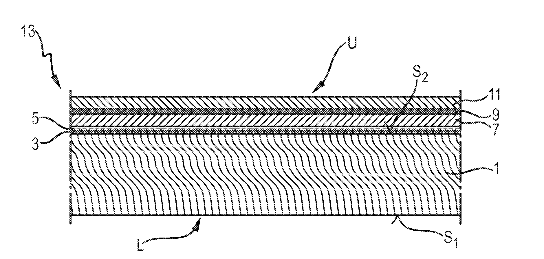
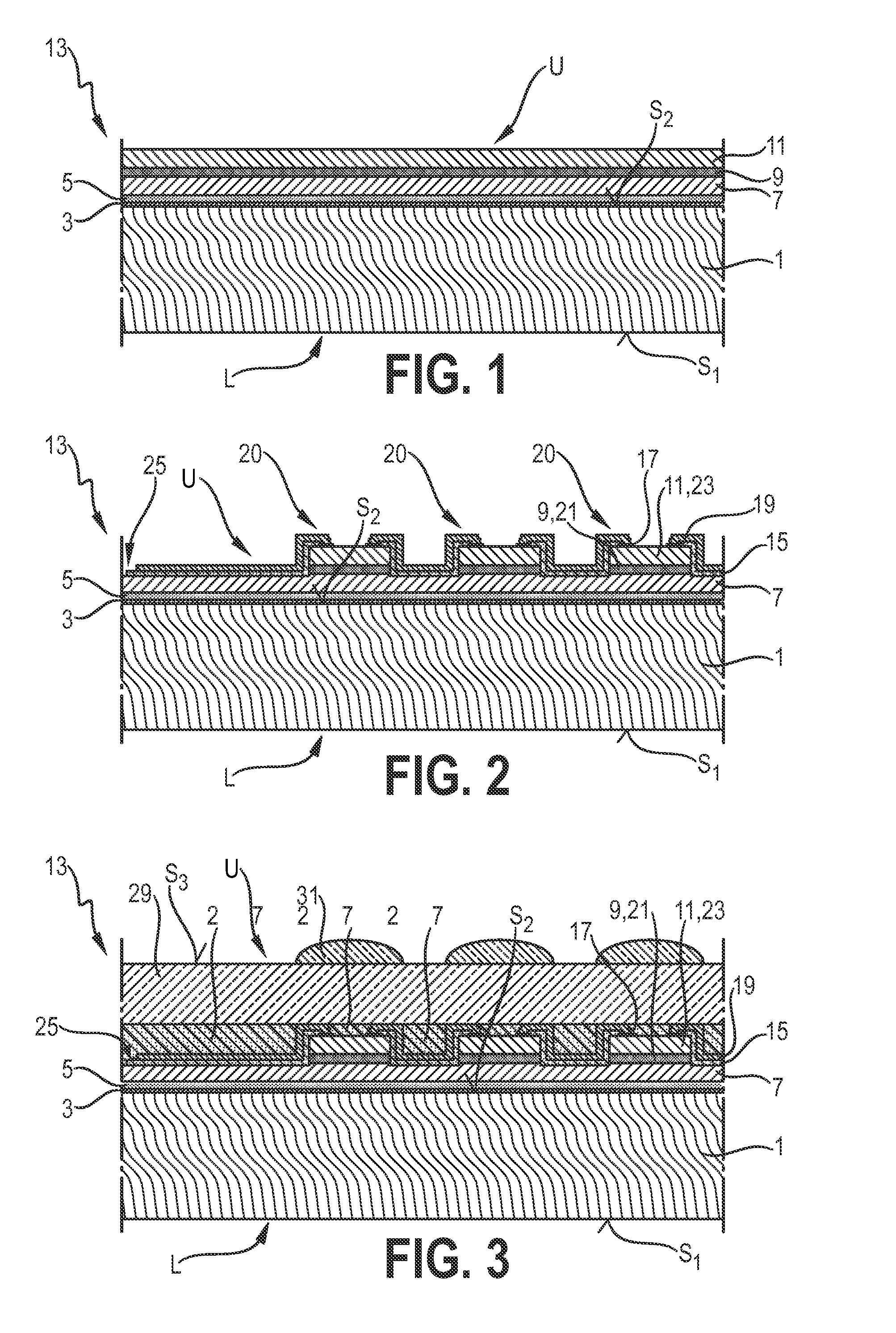
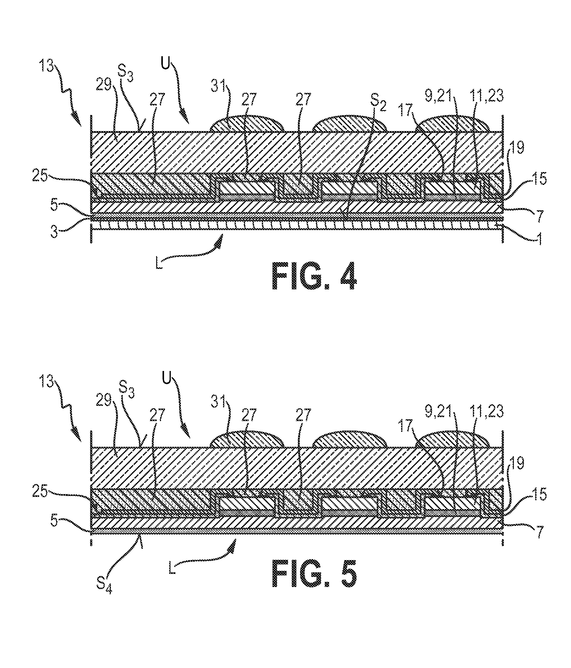
[0061]FIG. 1 shows a part of a semi-finished VCSEL product 13 for the production of a VCSEL chip, i.e. also for a VCSEL module, according to an embodiment of the invention.

[0062]The semi-finished VCSEL product 13 has an upper side U and a lower side L. It comprises in the given order from the lower side L to the upper side U: an intermediate substrate 1 with a first, lower, surface S1 and a second, upper, surface S2, an etch-stop layer 3 on the second surface S2, an electrically conductive buffer layer 5, a first doped layer plane 7, a light emitting layer plane 9 and a second doped layer plane 11. The first doped layer plane 7 and the second doped layer plane 11 will later function as mirrors to form the vertical cavity of the VCSEL chip. As they also need to serve as electrical contacts in this case they are made of layers with alternating refractive index, i.e. for instance GaAs or AlGaAs with thicknesses adapted to the emitted wavelength, for which purpose they are doped by Si a...


PUM


Abstract

The invention describes a method of manufacturing a VCSEL module (100) comprising at least one VCSEL chip (33) with an upper side (U) and a lower side (L) and with a plurality of VCSEL units (55) on a common carrier structure (35), the VCSEL units (55) comprising a first doped layer (50) of a first type facing towards the lower side (L) and a second doped layer (23) of a second type facing towards the upper side (U). The method comprises the steps of dividing the VCSEL chip (33) into a plurality of subarrays (39a, 39b, 39c, 39d, 39e, 39f, 39g, 39h, 39i) with at least one VCSEL unit (55) each, electrically connecting at least some of the subarrays (39a, 39b, 39c, 39d, 39e, 39f, 39g, 39h, 39i) in series. The invention also describes a VCSEL module (100) manufactured in such process.

Description

FIELD OF THE INVENTION[0001]The invention describes a method of manufacturing a VCSEL module comprising at least one VCSEL chip with an upper side and a lower side and with a plurality of VCSEL units on a common carrier structure, the VCSEL units comprising a first doped layer of a first type facing towards the lower side and a second doped layer of a second type facing towards the upper side. It also describes such VCSEL module.BACKGROUND OF THE INVENTION[0002]VCSEL modules are comprised of a number (i.e. one or a plurality) of VCSEL chips (also called dies) which chips comprise at least one, usually a large number of VCSEL units. The larger these chips the less mounting time and thus mounting costs for the production of VCSEL modules needs to be spent. Therefore, it is particularly beneficial to use as large semiconductor chips in this context as possible as long as they can be soldered with a good quality. Firstly, larger chips reduce the amount of lost wafer area due to sawing l...

Claims


Application Information

Patent Timeline
Patent Type & Authority Applications(United States)
IPC IPC(8): H01S5/42H01S5/00H01S5/40H01S5/183
CPCH01S5/423H01S5/4018H01S5/005H01S5/183H01S5/0216H01S5/0217H01S5/4025H01S5/02253
Inventor GRONENBORN, STEPHANPRUIJMBOOM, ARMANDDUMOULIN, RAIMOND LOUISMILLER, MICHAEL
Owner TRUMPF PHOTONIC COMPONENTS GMBH
Why Eureka
Try Eureka