Patterned opto-electrical substrate and method for manufacturing the same

a technology of opto-electronic substrates and patterned substrates, which is applied in the direction of semiconductor/solid-state device manufacturing, electrical apparatus, and semiconductor devices, etc., can solve the problems of reducing dislocation density or improving luminous efficiency, deteriorating the quality of epitaxial films, and reducing luminous efficiency, so as to improve the total reflectance and diffuse reflectance of substrates, improve the extraction efficiency of light-emitting diodes, and improve the total reflectance and diffuse refl

Active Publication Date: 2015-03-19
KINIK
View PDF6 Cites 29 Cited by
  • Summary
  • Abstract
  • Description
  • Claims
  • Application Information

AI Technical Summary

Benefits of technology

[0031]The present invention further proposes to use the spectrometer with an integrating sphere to measure the optical characteristics of the patterned substrate, and the pattern dimension (an outer diameter, a height or depth, and a spacing) of the patterned substrate is designed depending on two optical parameters: the total reflectance (a sum of a mirror reflectance and a diffuse reflectance) and the diffuse reflectance. In general, the patterned substrate with a higher diffuse reflectance may substantially improve the extraction efficiency of the light-emitting diode light. In the light emitting diode having a patterned opto-electrical substrate of the present invention, the total reflectance of the substrate may be arbitrarily changed according to the structure design of the first patterned structure or the second patterned structure, for example, alternation of the depth, height, outer diameter and spacing of the first patterned structure, or alternation of the depth or outer diameter of the second patterned structure, wherein the substrate may have a total reflectance of 30% or more, preferably 40% or more, more preferably 90% to 100%, and most preferably close to 100%. Furthermore, in the light emitting diode having a patterned opto-electrical substrate of the present invention, the diffuse reflectance of the substrate may be arbitrarily changed according to the structure design of the first patterned structure or the second patterned structure, for example, alternation of the depth, height, outer diameter and spacing of the first patterned structure, or alternatio...

Problems solved by technology

As a result, the GaN film can have a dislocation density up to 109 to 1010 cm−2, seriously deteriorating the quality of the epitaxial film, and the defects usually act as non-radiative recombination centers, resulting in a decreased luminous efficiency.
However, in the above-mentioned LEDs, the luminous efficiency thereof...

Method used


Image

  • Patterned opto-electrical substrate and method for manufacturing the same
  • Patterned opto-electrical substrate and method for manufacturing the same
  • Patterned opto-electrical substrate and method for manufacturing the same

Examples


example 1

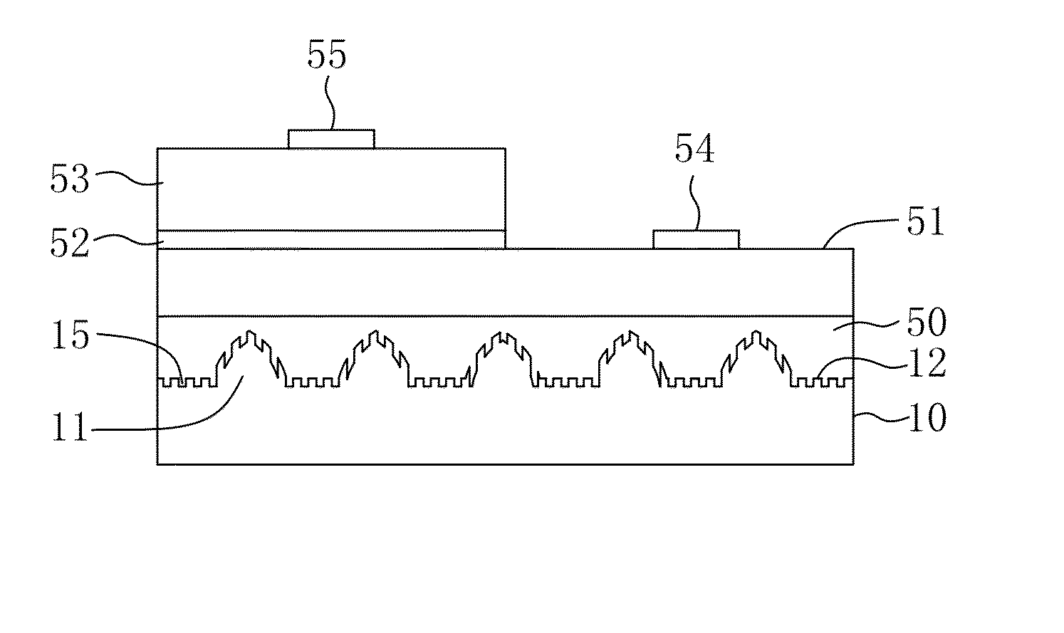
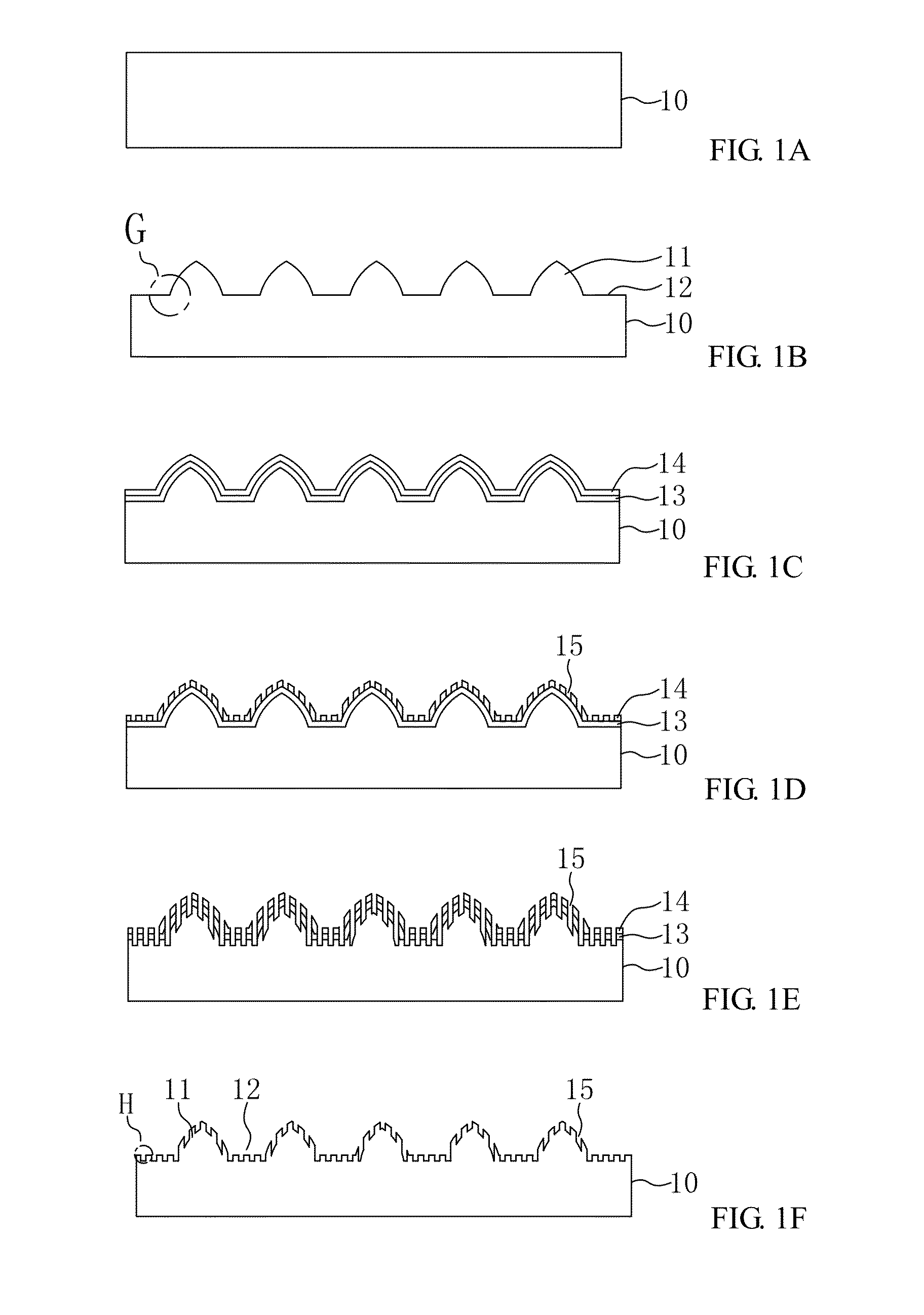
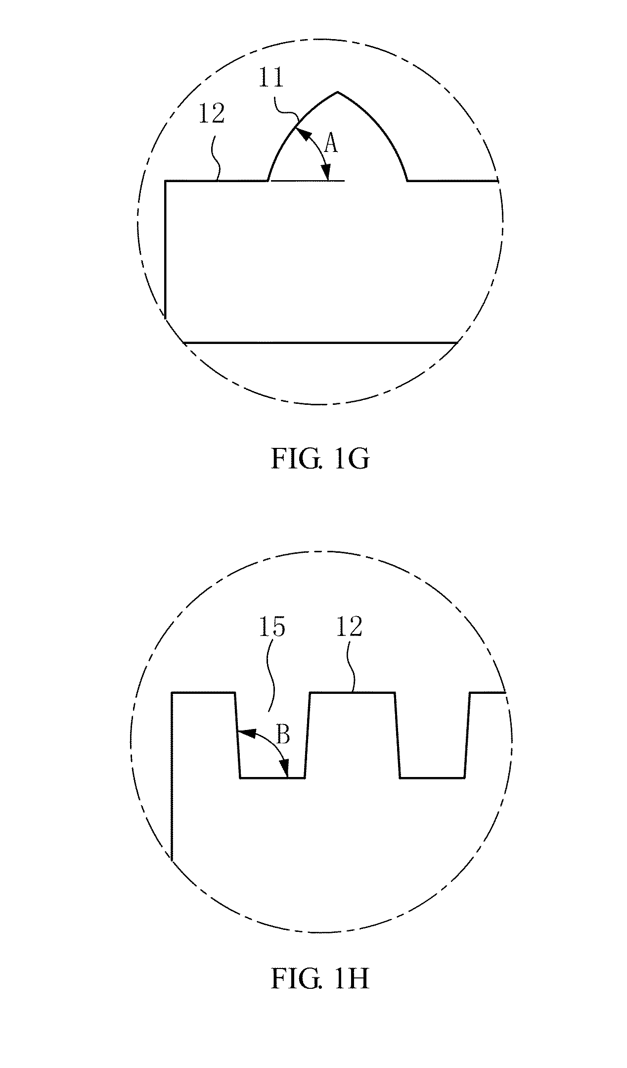
[0043]Refer to FIGS. 1A to 1H, which show the process flow for manufacture of the patterned opto-electrical substrate according to Example 1 of the present invention. First, referring to FIGS. 1A and 1B, a substrate 10 is provided. The substrate 10 is a sapphire substrate or a silicon substrate with a planar surface, and a first patterned structure 11 and a spacer region 12 are formed on a surface of the substrate 10 by a first etching treatment. In the first etching treatment, a first photoresist layer (not shown) is further disposed on a part of the surface of the substrate 10, so as to selectively remove a part of the substrate 10 by the first etching treatment, to form the micron-scale protruding first patterned structure 11 having a cone shape and the spacing region 12 of a planar structure. The first patterned structure 11 (i.e., the micron-scale protruding structure) has a height of 1.2 μm to 2 μm, an outer diameter of 1 μm to 5 μm, and a spacing between the two adjacent firs...

example 2

[0048]Refer to FIG. 2, which shows the schematic diagram of the patterned opto-electrical substrate according to Example 2 of the present invention. The patterned opto-electrical substrate and the manufacturing process thereof in Example 2 are substantially the same as in Example 1, except for the concave-convex profiles of the first patterned structures. Unlike Example 1, wherein the first patterned structure is the micron-scale protruding structure having a cone-shape (please also refer to FIG. 1B), in Example 2, a first photoresist layer (not shown) is provided on a part of the surface of the substrate 20, so as to selectively remove a part of the substrate 20 by the first etching treatment, to form the micron-scale recessing first patterned structure 21 having a cone shape and the spacing region 22 of a planar structure. Then, the same manufacturing process as in Example 1 is performed to provide the first patterned structure 21 with a plurality of the second patterned structure...

examples 3 to 5

[0049]Refer to FIG. 3A to 3C, which show the schematic diagrams of the patterned opto-electrical substrates according to Examples 3-5 of the present invention. The patterned opto-electrical substrate and the manufacturing process thereof in Examples 3-5 are substantially the same as in Example 1, except for the shapes of the first patterned structures.

[0050]Unlike Example 1, wherein the first patterned structure is the micron-scale protruding structure having a cone-shape (please also refer to FIG. 1B), referring to FIG. 3A, in Example 3, a first photoresist layer (not shown) is provided on a part of the surface of the substrate 301, so as to selectively remove a part of the substrate 301 by the first etching treatment, to form the micron-scale protruding first patterned structure 311 having a shape of triangular pyramid and the spacing region 321 of a planar structure. Then, the same manufacturing process as in Example 1 is performed to provide the first patterned structure 311 wit...


PUM


Abstract

The present invention relates to a patterned opto-electrical substrate, comprising a substrate, the substrate has a first patterned structure, a spacer region and a second patterned structure, wherein the second patterned structure is formed on one or both of the first patterned structure and the spacer region, and the first patterned structure is a micron-scale protruding structure or a micron-scale recessing structure, while the second patterned structure is a submicron-scale recessing structure. The present invention also relates to a method for manufacturing the aforementioned patterned opto-electrical substrate and light emitting diodes having the aforementioned patterned opto-electrical substrate.

Description

CROSS REFERENCE TO RELATED APPLICATION[0001]This application claims the benefits of the Taiwan Patent Application Serial Number 102133449, filed on Sep. 16, 2013, the subject matter of which is incorporated herein by reference.BACKGROUND OF THE INVENTION[0002]1. Field of the Invention[0003]The present invention relates to an opto-electrical patterned substrate and a manufacturing method thereof, and more particularly to a substrate having a first patterned structure of micron-scale and a second patterned structure of submicron-scale, and to a light-emitting diode having the same.[0004]2. Description of Related Art[0005]The development of human's lighting history has come to an era of solid-state lighting, and what is the common goal pursued in the industry of solid-state lighting is to provide a higher light-emitting brightness, cheaper price, longer life, and higher stability, and so on. The most important demand in the lighting market is the brightness of the light-emitting diode....

Claims


Application Information

Patent Timeline
IPC IPC(8): H01L33/22H01L33/12H01L33/32H01L33/00
CPCH01L33/22H01L33/007H01L33/32H01L33/12H01L33/002H01L21/0242H01L21/0243H01L33/005
Inventor KE, WEN-CHENGCHEN, WEI-KUOHOUNG, FWU-YIHHO, CHIA-CHE
Owner KINIK
Why Eureka
Try Eureka