

Substrate Processing Apparatus, Method of Manufacturing Semiconductor Device and Method of Processing Substrate
a technology of substrate and processing apparatus, which is applied in the direction of liquid surface applicators, coatings, chemical vapor deposition coatings, etc., can solve the problems of inability to low power consumption, and achieve high temperature recovery characteristics, rapid cooling of the insulating wall, and high temperature recovery characteristics
- Summary
- Abstract
- Description
- Claims
- Application Information
AI Technical Summary
Benefits of technology
Problems solved by technology
Method used
Image

Examples
first embodiment
1. First Embodiment
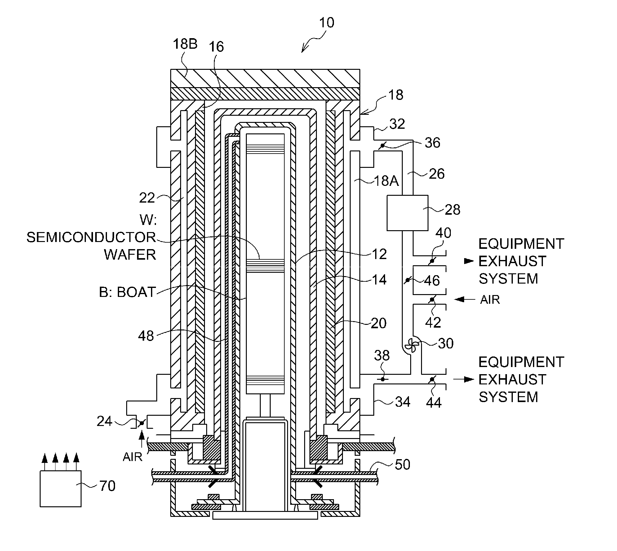
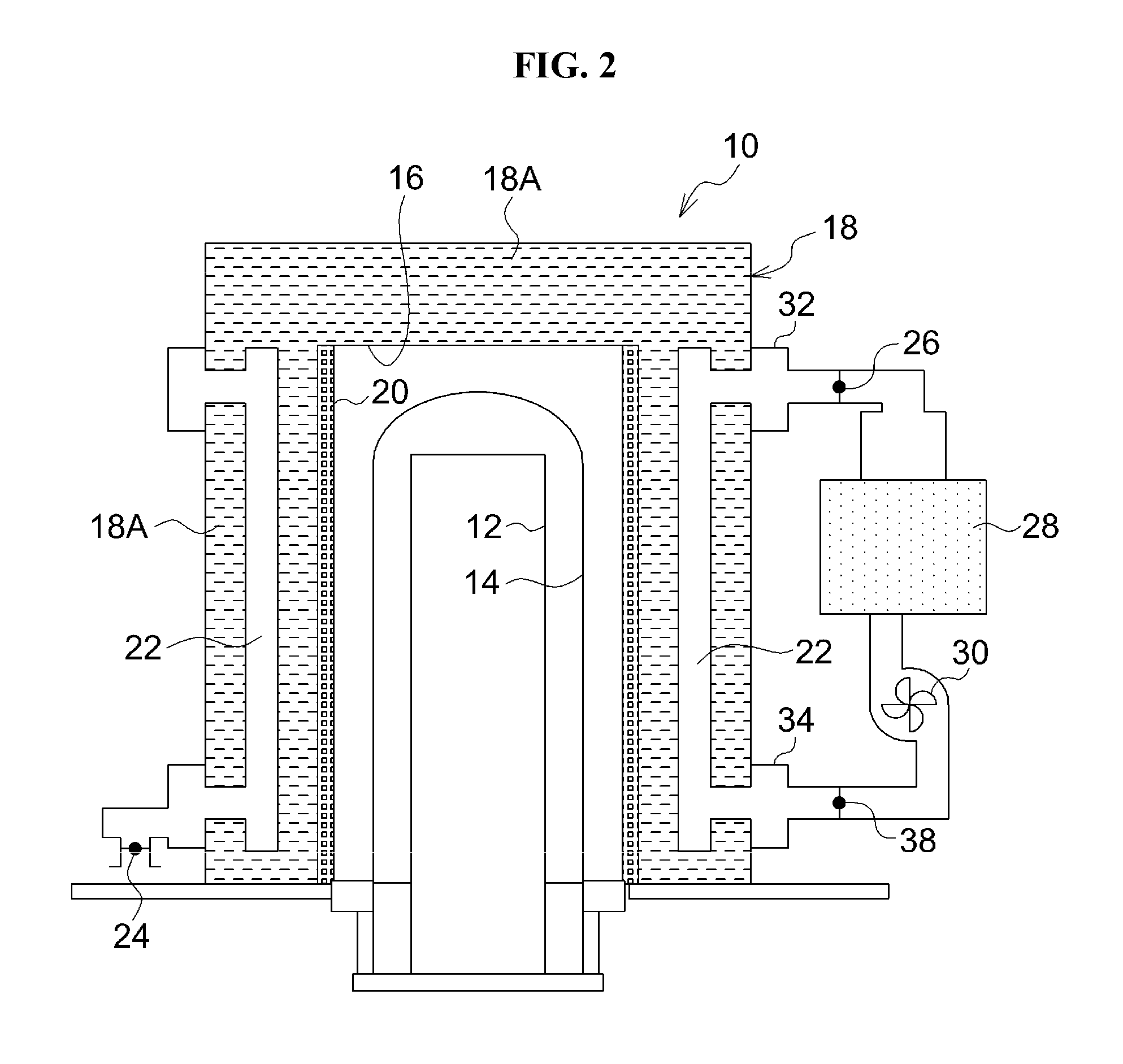
[0055]A substrate processing apparatus 10 according to one embodiment of the present invention will be hereinafter described with reference to the accompanying drawings.
[0056]
[0057]As illustrated in FIG. 1, the substrate processing apparatus 10 according to the first embodiment includes a reaction tube 12 having a vertical cylindrical shape (as an example of a reaction container) according to the present invention in which a boat B on which a semiconductor wafer W (as an example of a substrate) is placed is loaded; a liner tube 14 in which the reaction tube 12 is accommodated; an insulating wall 18 in which a reaction tube reception chamber 16 having a cylindrical shape (as an example of a reaction container accommodation chamber for accommodating the liner tube 14) is formed, and which includes a side surface insulating material 18A forming sidewall surfaces of the reaction tube reception chamber 16 and a ceiling surface insulating material 18B forming a ceiling ...
second embodiment
2. Second Embodiment
[0086]A substrate processing apparatus according to another embodiment of the present invention will be described with reference to the accompanying drawings below. In FIGS. 5 to 9, reference numerals that are the same as those in FIGS. 1 to 4B denote the same elements as those in FIGS. 1 to 4B except for a special case.
[0087]
[0088]As illustrated in FIG. 5, in a substrate processing apparatus 110 according to the present invention, a space between an inner wall surface of an side surface insulating material 18A and a liner tube 14 is used as a rapid cooling channel 52, and a communication flow channel 54 communicating the rapid cooling channel 52 and an air circulation channel 22 passes through a portion of a wall surface of the side surface insulating material 18A between the air circulation channel 22 and the rapid cooling channel 52 and a heater 20.
[0089]A rapid cooling exhaust channel 56 is installed at a ceiling surface insulating material 18B. The rapid coo...
third embodiment
3. Third Embodiment
[0105]A third embodiment of the present invention will be described with reference to FIGS. 10A and 10B. In the third embodiment of FIGS. 10A and 10B, an air circulation channel 102B is further installed in a ceiling surface insulating material 18B, as well as a side surface insulating material 18A, compared to the first embodiment of FIG. 2 in which the air circulation channel 22 is installed in the side surface insulating material 18A. Also, in FIGS. 10A and 10B, reference numerals that are the same as those in FIGS. 1 to 3C denote the same elements as those illustrated in FIGS. 1 to 3C except for a special case.
[0106]FIGS. 10A and 10B illustrate examples of an air circulation channel of a substrate processing apparatus according to the third embodiment. FIG. 10A illustrates a case that an air circulation channel 102A installed in the side surface insulating material 18A and the air circulation channel 102B installed in the ceiling surface insulating material 18...
PUM
| Property | Measurement | Unit |
|---|---|---|
| temperature | aaaaa | aaaaa |
| cylindrical shape | aaaaa | aaaaa |
| heat radiation property | aaaaa | aaaaa |
Abstract
Description
Claims
Application Information