Field Programmable Gate-Array with Embedded Network-on-Chip Hardware and Design Flow

a technology of network-on-chip hardware and gate array, applied in the field of fieldprogrammable gate array, can solve the problems of increasing logic speed and increasing timing closure challenges for long distance communication, and achieve the effects of improving system-level interconnection efficiency, simplifying and more automated design integration of large systems

Inactive Publication Date: 2015-04-23
VAUGHN TIMOTHY BETZ +1
View PDF2 Cites 123 Cited by
  • Summary
  • Abstract
  • Description
  • Claims
  • Application Information

AI Technical Summary

Benefits of technology

[0012]Changes to the FPGA design flow to target NoCs may be divided into two categories; logical design and physical design. The logical design step concerns the functional design of the implemented system. In the logical design step all or part of the designed system is made latency-insensitive by adding wrappers to the modules. The logical design step also includes generating the required interfaces to connect modules to an NoC and programming the NoC for use. Programming the NoC includes, but is not limited to the following: configuring the routers, assigning priorities to data classes, as...

Problems solved by technology

Logic speeds are increasing more than metal speeds, presenting ...

Method used


Image

  • Field Programmable Gate-Array with Embedded Network-on-Chip Hardware and Design Flow
  • Field Programmable Gate-Array with Embedded Network-on-Chip Hardware and Design Flow
  • Field Programmable Gate-Array with Embedded Network-on-Chip Hardware and Design Flow

Examples


Embodiment Construction

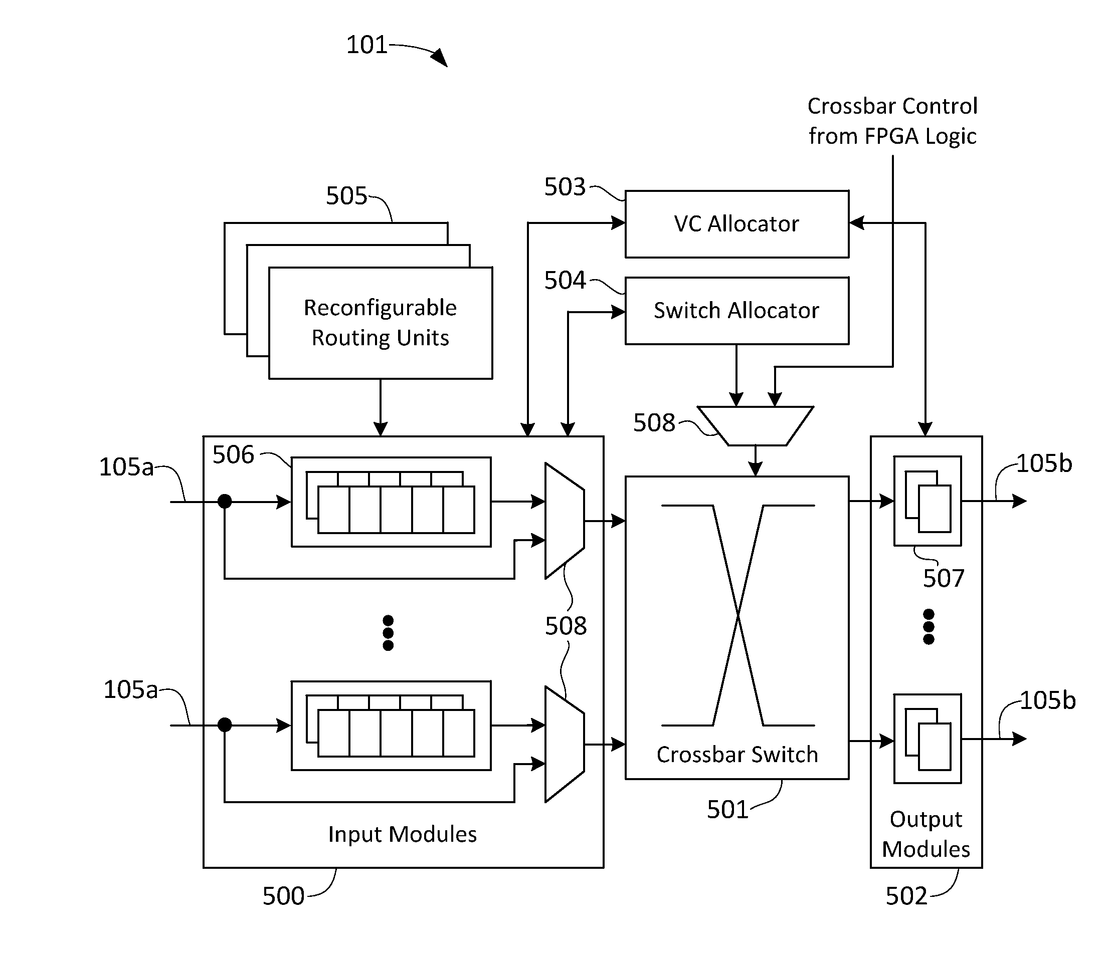
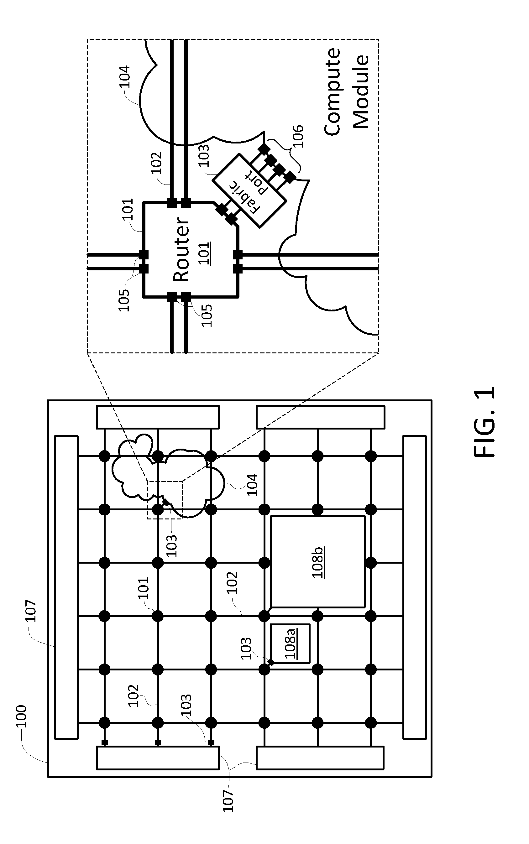
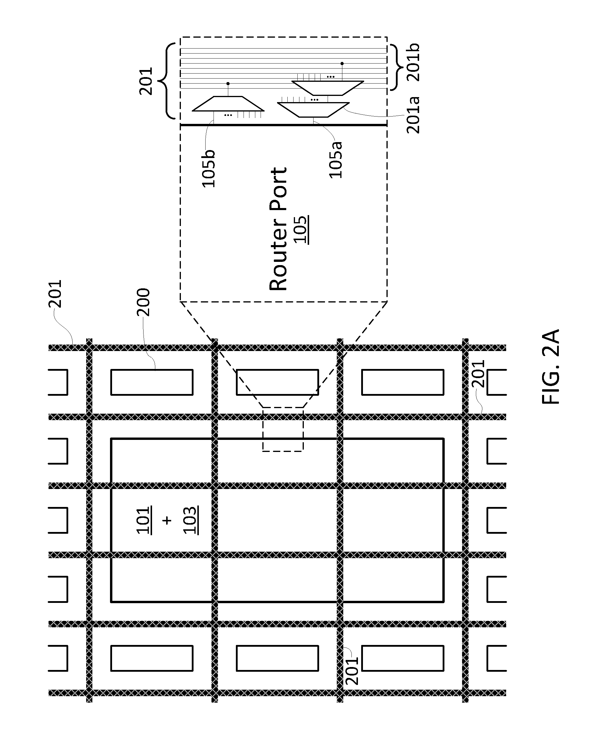
[0021]Reference will now be made in detail to some specific examples of the invention including the best modes contemplated by the inventors for carrying out the invention. Examples of these specific embodiments are illustrated in the accompanying drawings. While the invention is described in conjunction with these specific embodiments, it will be understood that it is not intended to limit the invention to the described embodiments. On the contrary, it is intended to cover alternatives, modifications, and equivalents as may be included within the spirit and scope of the invention as defined by the appended claims.

[0022]For example, the apparatus and techniques of the present invention will be described in the context of FPGAs. However, it should be noted that the techniques of the present invention can be applied to other programmable chips similar to FPGAs or based on them. In the following description, numerous specific details are set forth in order to provide a thorough underst...


PUM


Abstract

An enhanced field programmable gate-array (FPGA) incorporates one or more programmable networks-on-chip (NoCs) or NoC components integrated within the FPGA fabric. This NoC interconnect augments the existing FPGA interconnect. In one embodiment, the NoC is used as system-level interconnect to connect compute and communication modules to one another and integrate large systems on the FPGA. The NoC components include a “fabric port”, which is a configurable interface that bridges both data width and frequency between the embedded NoC routers and the FPGA fabric components such as logic blocks, block memory, multipliers, processors or I/Os. Finally, the FPGA design flow is modified to target the embedded NoC components either manually through designer intervention, or automatically.

Description

FIELD OF THE INVENTION[0001]The invention relates to Field-Programmable Gate-Arrays (FPGAs) or other programmable logic devices (PLDs) or other devices based thereon. Specifically, the addition of networks-on-chip (NoC) to FPGAs. This includes both modifications to the FPGA architecture and design flow.BACKGROUND[0002]This invention relates to FPGAs and more particularly to a new interconnect architecture for such devices.[0003]FPGAs are a widely-used form of integrated circuit due to the flexibility provided by their customizable nature. FPGAs consist primarily of programmable logic blocks, programmable inputs and outputs (I / Os) and programmable interconnect. Traditionally, logic blocks are organized into a 2 dimensional array and these logic blocks are surrounded by programmable interconnect wires and multiplexers.[0004]An FPGA's programmable logic blocks traditionally consist of a plurality of lookup tables, multiplexers and flip flops or latches. Lookup tables typically consist ...

Claims


Application Information

Patent Timeline
IPC IPC(8): G06F17/50H03K19/0175
CPCH03K19/017581G06F17/5054G06F30/34
Inventor ABDELFATTAH, MOHAMED SAIEDBETZ, VAUGHN TIMOTHY
Owner VAUGHN TIMOTHY BETZ
Why Eureka
Try Eureka