
Eureka
For R&D, Eureka makes reading and utilizing patents & technical documents easy.
Eureka AIR
Designed for self-driven R&D workflows. Generate viable solutions, solve complex R&D challenges, empower your innovation with AI.

Eureka Materials
Designed for material experts only. Revolutionize your material R&D, from search, analyze, to developing new materials.

TechResearch
Generate reliable direction feasibility study reports for your R&D in just a few steps.

TechSeek
Discover and master advanced knowledge NOW. Basics, ideas, possibilities, all at once.

TechMind
As an expert in R&D Theories, TechMind can generates customized viable solutions instantly.

TechRisk
Analyze your overall solution with one click, know your potential R&D risks in advance.

TechMonitor
Get weekly tech updates, stay abreast of the latest tech innovations and key insights.
Electronic device and metal thin film-provided spacer
- Summary
- Abstract
- Description
- Claims
- Application Information
AI Technical Summary
Benefits of technology
Problems solved by technology
Method used
Image

Examples
embodiment 1
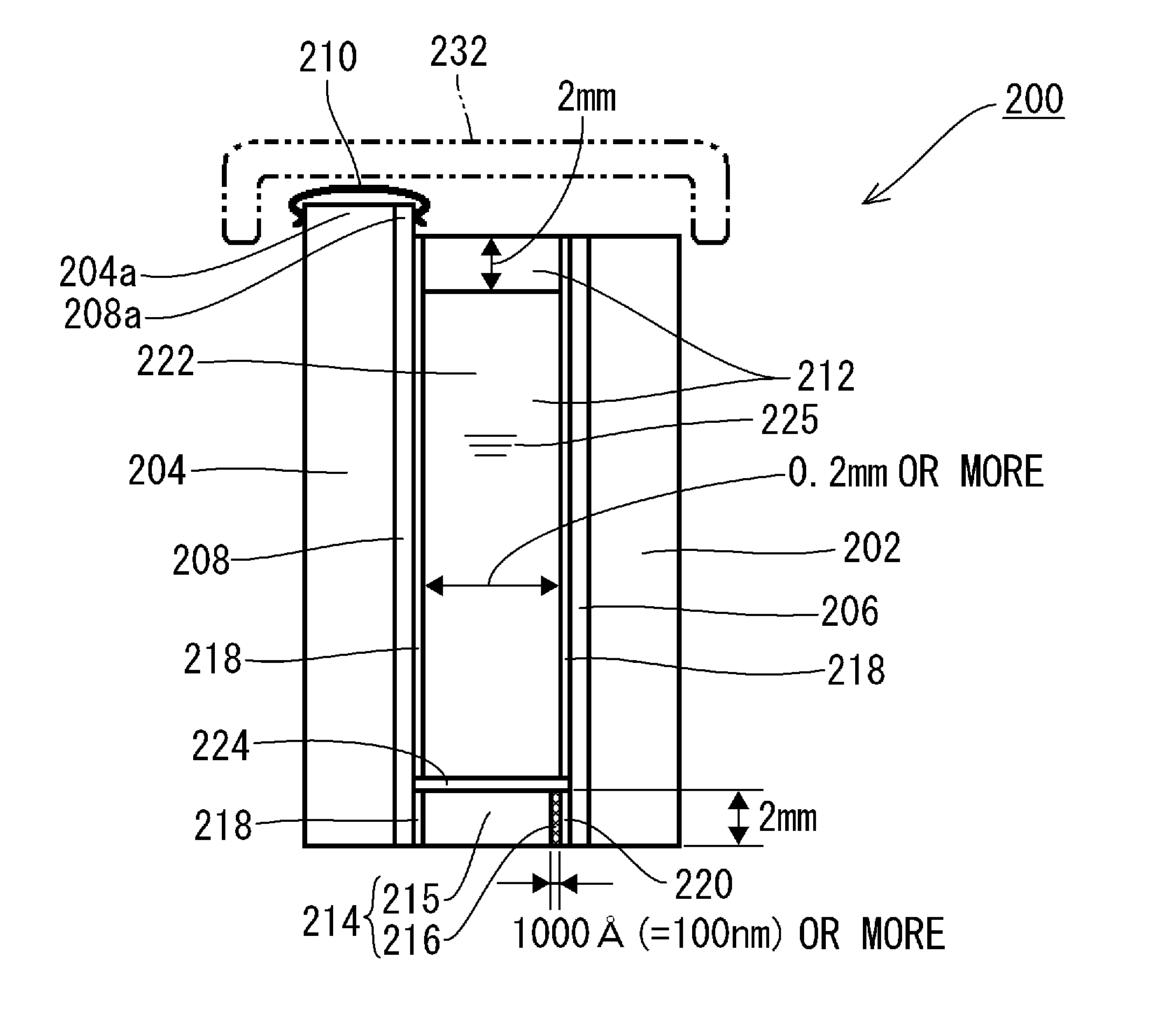
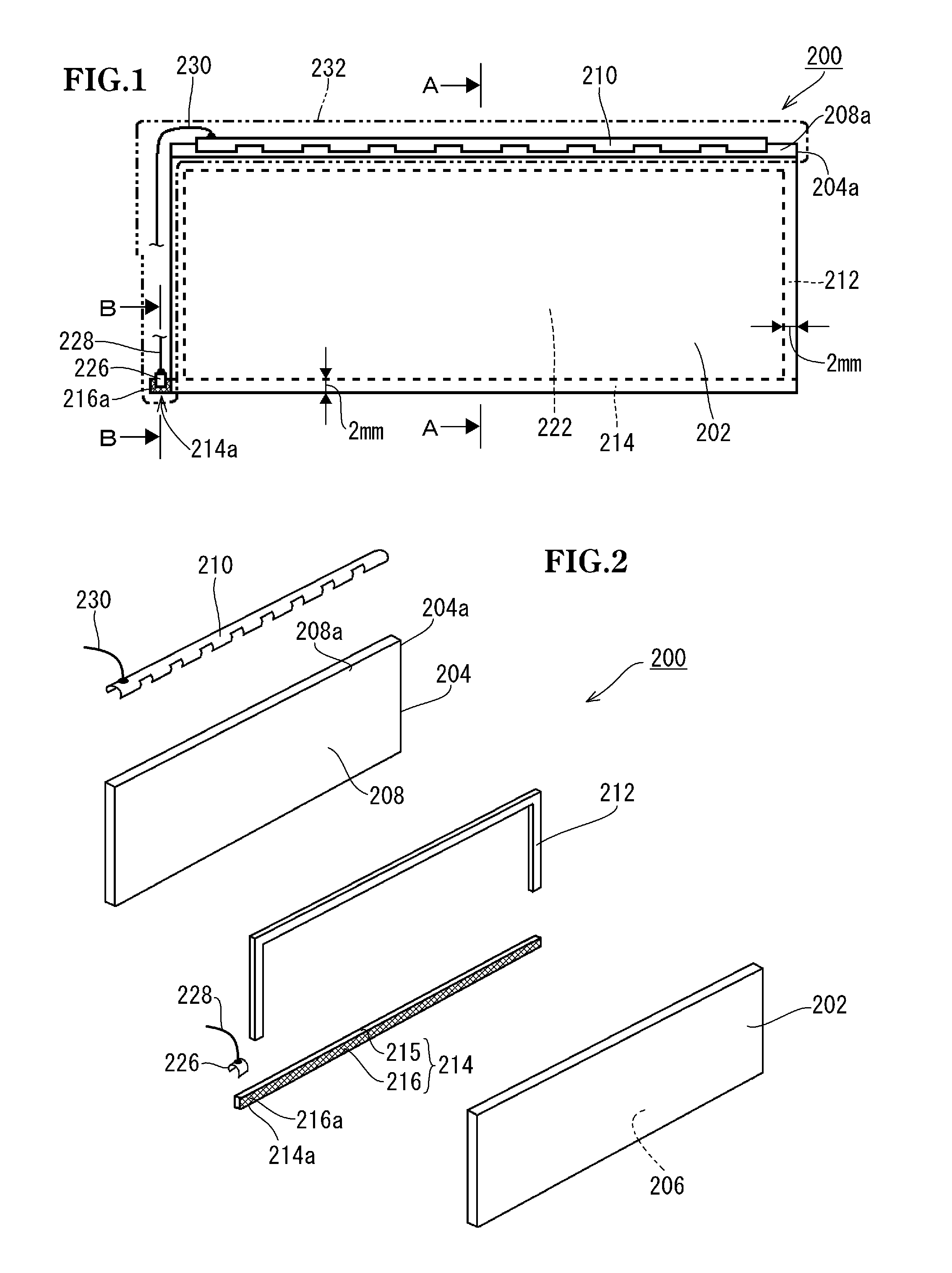
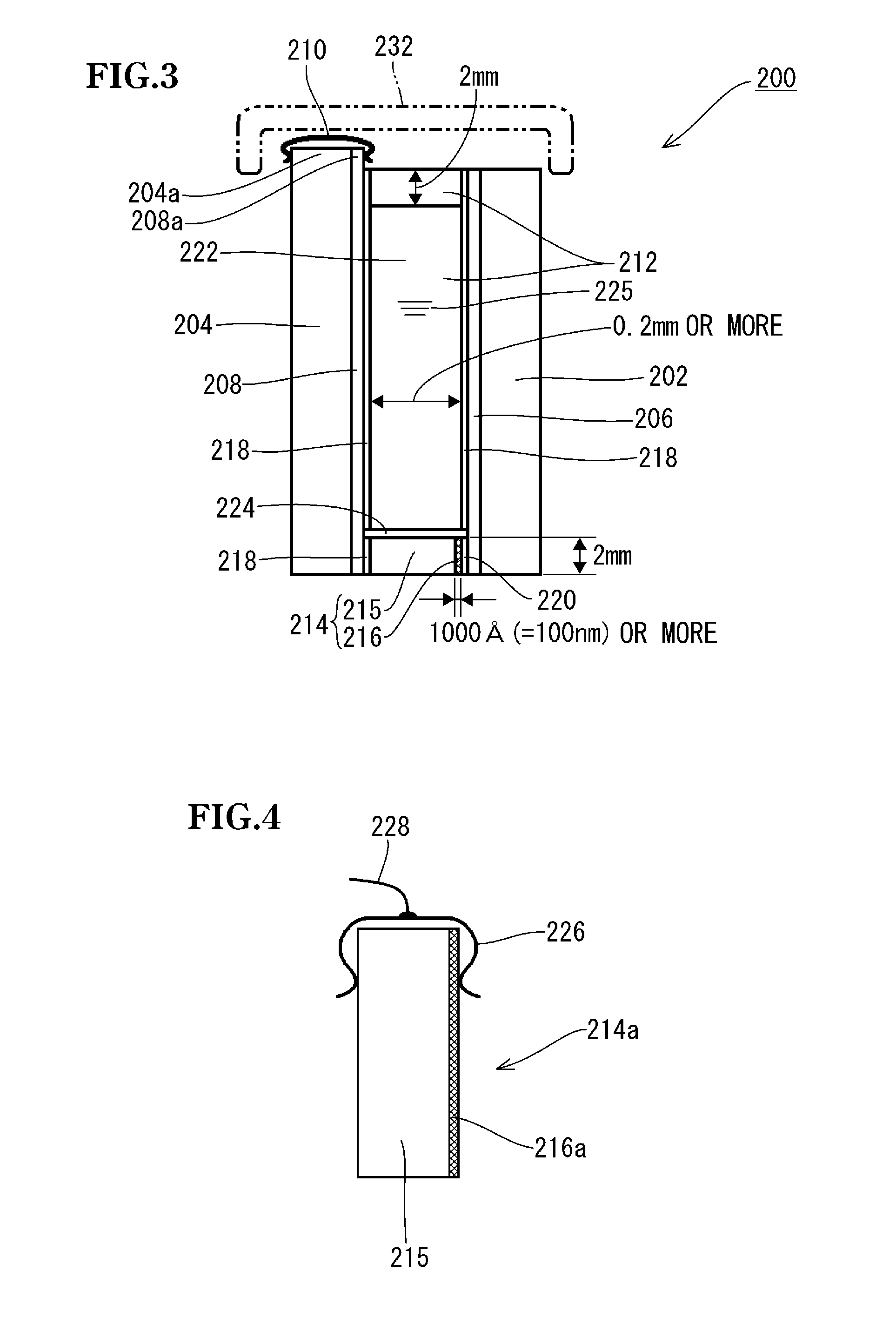
[0036]FIGS. 1 to 4 illustrate Embodiment 1 of an electronic device according to the present invention. In this embodiment, an electronic device according to the present invention is configured as a transmissive element. The transmissive element can be used as, for example, an electrochromic or liquid-crystal building dimming window, an electrochromic vehicle dimming window, electrochromic dimming glasses or an electrochromic vehicle sun visor device, which is described later as an example application. Here, a bus bar is formed using a metal thin film-provided spacer according to the present invention for one of respective electrode films formed on two substrates, and a bus bar is formed using a conventional clip electrode for the other electrode film. As illustrated in the front view in FIG. 1, an electronic device 200 has a front shape of a horizontally-long rectangle. As illustrated in the exploded perspective view in FIG. 2, the electronic device 200 includes a front-side transpa...
embodiment 2
[0044]FIGS. 6 to 8 illustrate Embodiment 2 of the present invention. In this embodiment, an electronic device according to the present invention is configured as an electrochromic vehicle inner mirror. Here, bus bars are formed for respective electrode films formed on two substrates, using (two) separate metal thin film-provided spacers according to the present invention. For parts corresponding to those of Embodiment 1, reference numerals that are the same as those of Embodiment 1 are used. In an inner mirror 234, substrates 202 and 204 have same dimensions in a long direction and a short direction. While the substrate 202 is transparent, the substrate 204 does not have to be transparent. From among facing surfaces of the substrates 202 and 204, on the transparent substrate 202 side, a transparent electrode film 206 is formed using a film forming technique such as sputtering or vapor deposition, and on the substrate 204 side, an electrode and reflection film 238 of a metal thin fil...
embodiment 3
[0050]FIGS. 9 to 12 illustrate Embodiment 3 of the present invention. In this embodiment, an electronic device according to the present invention is configured as an electrochromic vehicle inner mirror. Here, bus bars are formed for respective electrode films of two substrates, using a common (single) metal thin film-provided spacer according to the present invention. In other words, metal thin films 216 and 246 are formed on both surfaces, i.e., a front surface and a back surface, of a metal thin film-provided spacer 214′ disposed at a lower side of an inner mirror 256 so as to be not conductively connected to each other. For parts corresponding to those of Embodiments 1 and 2, reference numerals that are the same as those of Embodiments 1 and 2 are used. In the inner mirror 256, substrates 202 and 204 have same dimensions in a long direction and a short direction. While the substrate 202 is transparent, the substrate 204 does not have to be transparent. From among facing surfaces ...
PUM
 Abstract
Description
Claims
Application Information
 - R&D Engineer
- R&D Manager
- IP Professional
- Industry Leading Data Capabilities
- Powerful AI technology
- Patent DNA Extraction
Browse by: Latest US Patents, China's latest patents, Technical Efficacy Thesaurus, Application Domain, Technology Topic, Popular Technical Reports.
© 2024 PatSnap. All rights reserved.Legal|Privacy policy|Modern Slavery Act Transparency Statement|Sitemap|About US| Contact US: help@patsnap.com