

Atomic layer removal process with higher etch amount
a technology of atomic layer and etching amount, which is applied in the direction of basic electric elements, semiconductor/solid-state device manufacturing, electric apparatus, etc., can solve the problems of increasing the effectiveness of “reset”, limiting the amount of material that may be etched per cycle, and increasing the total process time. , to achieve the effect of improving the overall etch rate and throughput of the alr etch process, excellent process control, and limiting the amount of material
- Summary
- Abstract
- Description
- Claims
- Application Information
AI Technical Summary
Benefits of technology
Problems solved by technology
Method used
Image

Examples
Embodiment Construction
Introduction
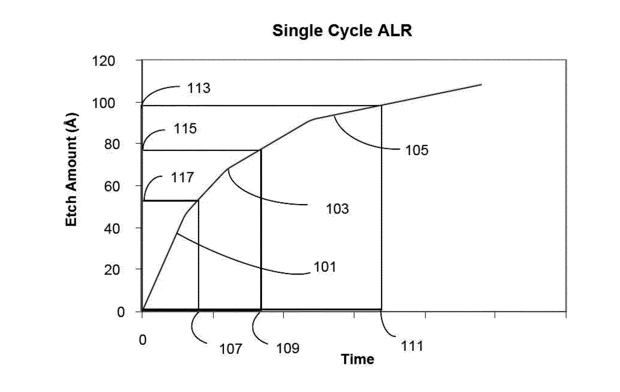
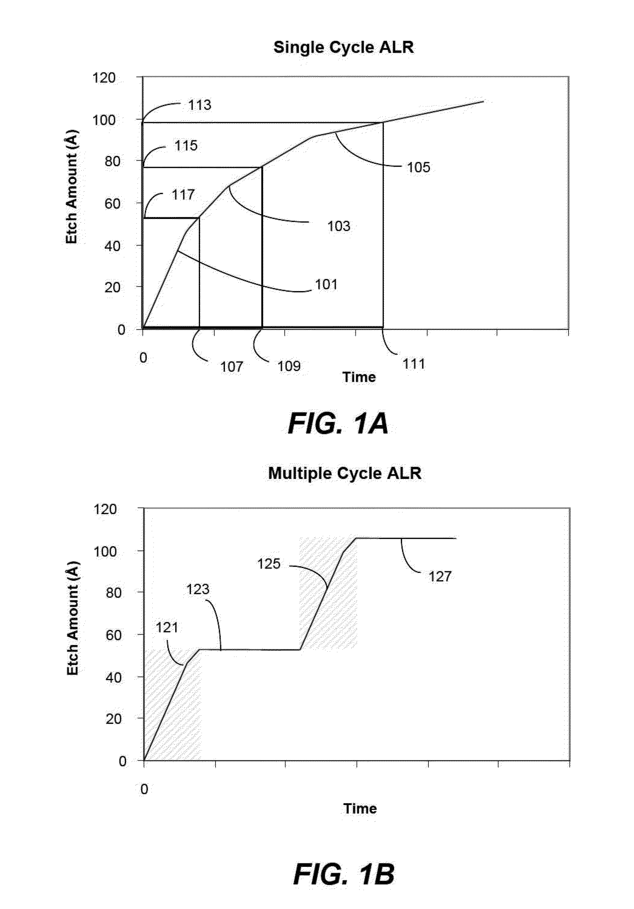
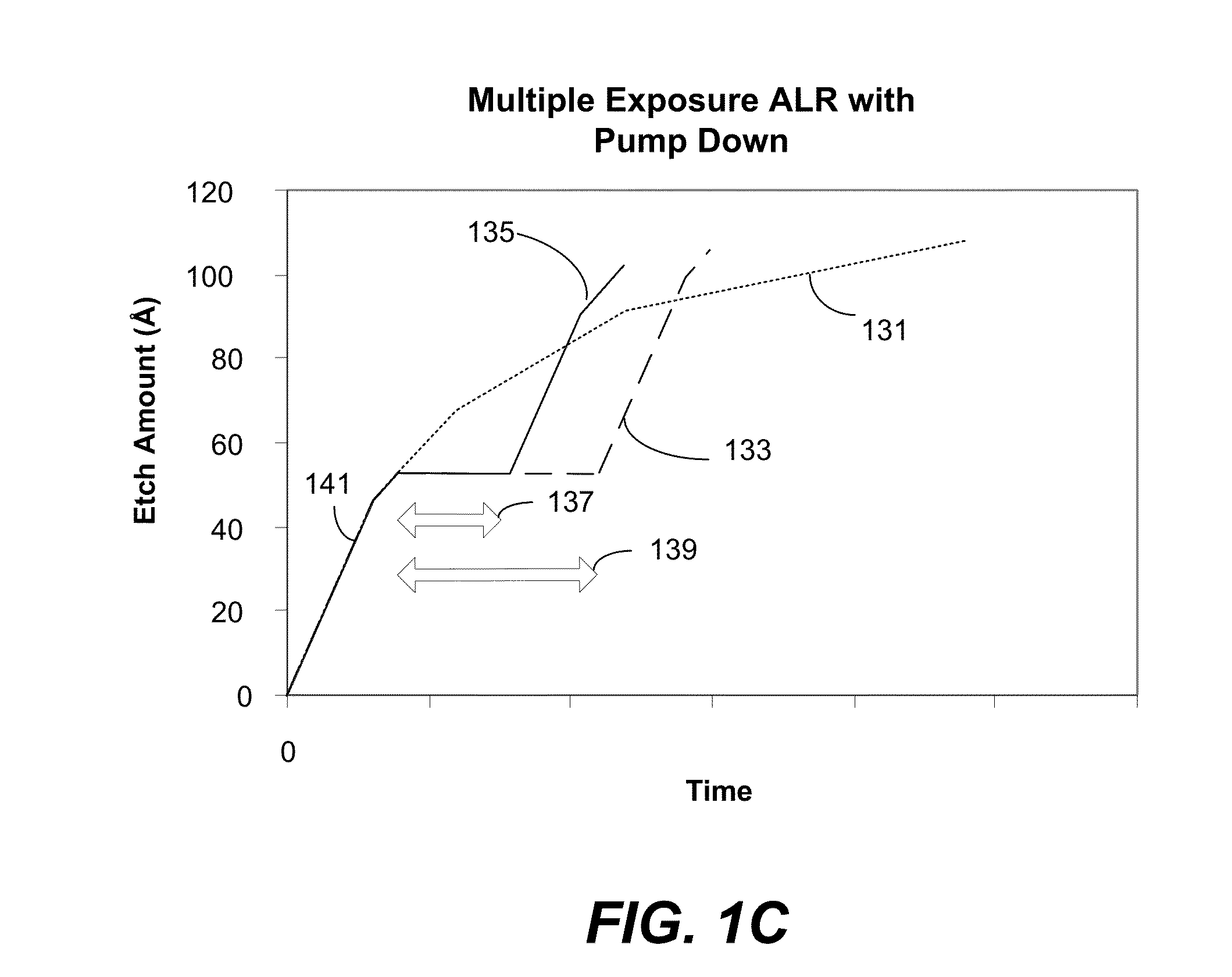
[0025]Embodiments of the present invention are described herein in the context of etching a substrate with blanket dielectric film and the context of filling a gap with dielectric material. Those of ordinary skill in the art will realize that the following detailed description of the present invention is illustrative only and is not intended to be in any way limiting. Other embodiments of the present invention will readily suggest themselves to such skilled persons having the benefit of this disclosure. For example, the gap fill application may be for shallow trench isolation (STI), inter-layer dielectric (ILD), inter-metal dielectric (IMD), or pre-metal dielectric (PMD).
[0026]Reference will be made in detail to implementations of the present invention as illustrated in the accompanying drawings. The same reference indicators will be used throughout the drawings and the following detailed description to refer to the same or like parts. In this application, the terms “wor...
PUM
 Abstract
Description
Claims
Application Information