
Inspection system

a technology of inspection system and inspection circuit, which is applied in the field of inspection system, can solve the problems of gate oxide film breakage, wire insulation failure, and short circuit of wiring, and achieve the effect of improving the sensitivity of defect detection and reducing diffraction ligh

Active Publication Date: 2015-05-14
HITACHI HIGH-TECH CORP
View PDF15 Cites 7 Cited by
  • Summary
  • Abstract
  • Description
  • Claims
  • Application Information

AI Technical Summary

Benefits of technology

The present invention has the technical effect of reducing stray light when inspecting objects using a spatial filter. This improves the sensitivity of defect detection. Additionally, the invention automatically adjusts the width of the spatial filter, making it more efficient in detecting defects.

Problems solved by technology

In the semiconductor manufacturing process, fine particles on the semiconductor substrate contribute to an insulation failure of wiring and a short circuit of wiring.
Along with the progress of miniaturization of patterns on semiconductor devices, minute particles on a semiconductor substrate contribute to an insulation failure of a capacitor, breakage of a gate oxide film, etc.
As miniaturization of the patterns on the semiconductor devices are progressed, smaller particles or smaller defects may contribute to a failure of semiconductor devices.

Method used


Image

  • Inspection system
  • Inspection system
  • Inspection system

Examples


first embodiment

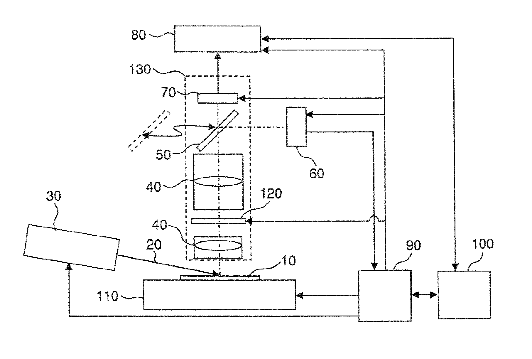
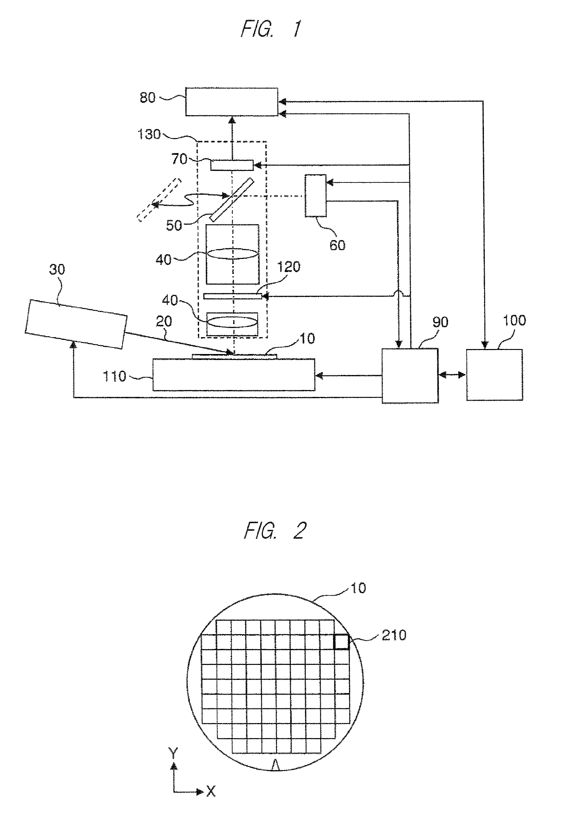
[0028]FIG. 1 is an overall block diagram of an inspection system of the present embodiment. An object to be inspected 10 (such as specimen, substrate, wafer, etc.) is mounted on a stage 110. The stage 110 is configured by combining an XY stage, a Z stage, a rotating stage, etc. Although various configurations are used as the stage 110, it is preferable that the stage 110 is capable of scanning the object to be inspected 10 in an XY plane so as to enable an inspection optical system 130 installed above the stage 110 to inspect the whole surface of the object to be inspected 10.

[0029]The object to be inspected 10 is irradiated with illumination light 20 emitted from an illumination optical system 30 (including light source). Parts of scattering light from a defect (such as particle and defect in a pattern) on the object to be inspected 10 are incident on a detection lens 40, and guided into a sensor 70 through a beam splitter 50 disposed immediately before an image surface of the dete...

second embodiment

[0066]Next, a second embodiment will be described. In the first embodiment, the example in which one inspection optical system 130 is used has been described. The present embodiment differs from the first embodiment in that a plurality of inspection optical systems are used. Hereinafter, the present embodiment will be described in details. In particular, the parts different from those of the first embodiment will be mainly described.

[0067]FIG. 13 is a diagram explaining an inspection system of the present embodiment. The inspection system of present embodiment includes an upper inspection optical system 1110 disposed in a normal direction of the object to be inspected 10, a first oblique inspection optical system 1120 disposed at a first elevation angle with respect to the object to be inspected 10, and a second oblique inspection optical system 1130 disposed at a second elevation angle with respect to the object to be inspected 10. Each of the upper inspection optical system 1110, ...


PUM

PropertyMeasurementUnit
widthaaaaaaaaaa
sizesaaaaaaaaaa
widthaaaaaaaaaa

Abstract

To improve sensitivity of a defect inspection, it is required to decrease influence of excessive diffraction from a spatial filter. Further, it is preferable to secure signal intensity from defects and particles as much as possible, while the influence of the excessive diffraction is decreased as much as possible. The present invention is characterized in setting a width of a spatial filter surface such that an unnecessary image caused by diffraction, that is, an intensity of the excessive diffraction is sufficiently small with respect to an intensity of a desired image. In the present invention, an SN ratio that is an index for deciding a width of the spatial filter is calculated from a region subjected to the influence of the excessive diffraction in an inspection image, and a width of a shield unit of the spatial filter is set so as to maximize the SN ratio.

Description

TECHNICAL FIELD[0001]The present invention relates to an inspection system. The present invention relates to, more particularly, an inspection system and an inspection method that detect a defect on a substrate on which a circuit pattern in a semiconductor manufacturing process is formed, and a spatial filter control apparatus and a spatial filter setting method used in the inspection system and the inspection method.BACKGROUND ART[0002]In a semiconductor manufacturing process, in order to promote a yield ratio, an inspection process is set in various steps during the semiconductor manufacturing process, and particles on a semiconductor substrate, defects in a formed pattern, etc. are inspected. In the semiconductor manufacturing process, fine particles on the semiconductor substrate contribute to an insulation failure of wiring and a short circuit of wiring. Along with the progress of miniaturization of patterns on semiconductor devices, minute particles on a semiconductor substrat...

Claims


Application Information

Patent Timeline
Patent Type & Authority Applications(United States)
IPC IPC(8): G01N21/88G01N21/95
CPCG01N21/8806G01N21/8851G01N2201/068G01N2201/06113G01N2201/12G01N21/9501G01N21/95623G01N21/95684
Inventor OHTSUBO, KENSHIRONISHIYAMA, HIDETOSHIJINGU, TAKAHIROITO, MASAAKI
Owner HITACHI HIGH-TECH CORP
Learn More