Defect inspection method and apparatus therefor

a defect detection and apparatus technology, applied in the field of pattern inspection and foreign substance inspection technology, can solve the problems of high na reaching the physical critical limit, the method of scanning on a sample by fine laser beam cannot be used, and the resolution limit of the image-forming optical system is the pattern width, etc., to achieve the effect of increasing the defect detection sensitivity, high efficiency and prolonging the life of the laser sour

Inactive Publication Date: 2005-04-21
HITACHI LTD
View PDF23 Cites 7 Cited by
  • Summary
  • Abstract
  • Description
  • Claims
  • Application Information

AI Technical Summary

Benefits of technology

[0011] In addition, a plurality of laser beams are used as light sources, because it is possible to expect not only the increase of the defect detection sensitivity, but also other various effects such as long life and countermeasure against breakdown. Also, laser beams of different wavelengths are used and combined because they are effective for controlling the polarized state. Since each laser output can also be reduced, the life of the laser sources can be extended. The addition of laser beams is made by use of a polarization beam splitter, dichroic mirror or half mirror.
[0012] The beams of the same wavelength can be processed, by a polarization beam splitter, to be laser beams of which the polarization directions are perpendicular to each other. The dichroic mirror is able to change the polarization directions of laser beams of different wavelengths to parallel or orthogonal directions. As compared with the half mirror, those processes can be achieved with high efficiency. In addition, the polarized state of one or both of different-wavelength beams can be changed by use of a wave plate.

Problems solved by technology

This pattern width is the resolution limit of the image-forming optical system.
However, the high NA has reached the physical critical limit.
Moreover, since the inspection is required to be fast conducted, the method of scanning on a sample by fine laser beam cannot be used.
If the laser beam is spread out up to full field of view in order to illuminate at a time, speckles occur, and overshoot and undershoot called ringing are caused at the edges of the circuit pattern, thus degrading the picture quality.

Method used


Image

  • Defect inspection method and apparatus therefor
  • Defect inspection method and apparatus therefor
  • Defect inspection method and apparatus therefor

Examples


Embodiment Construction

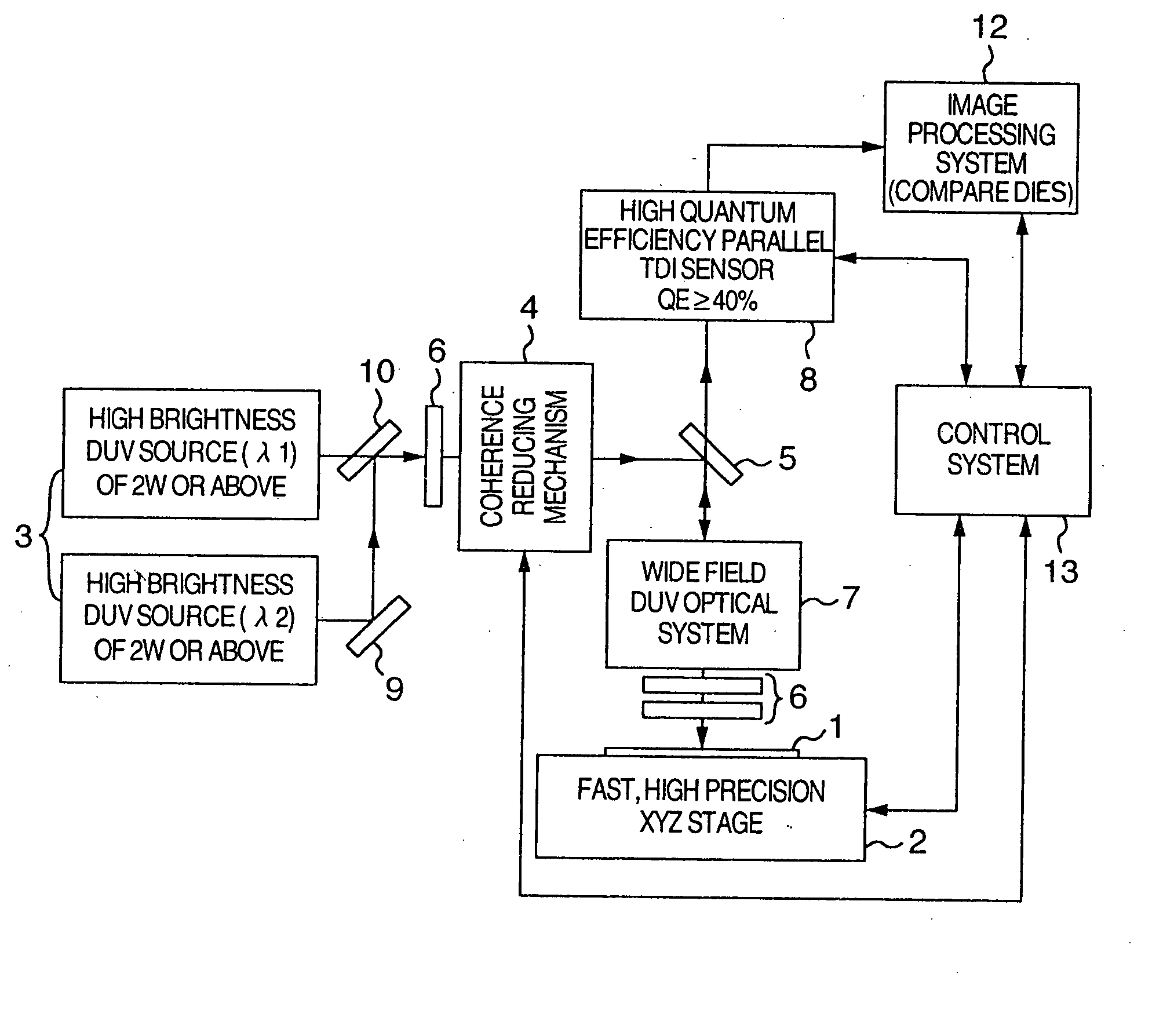
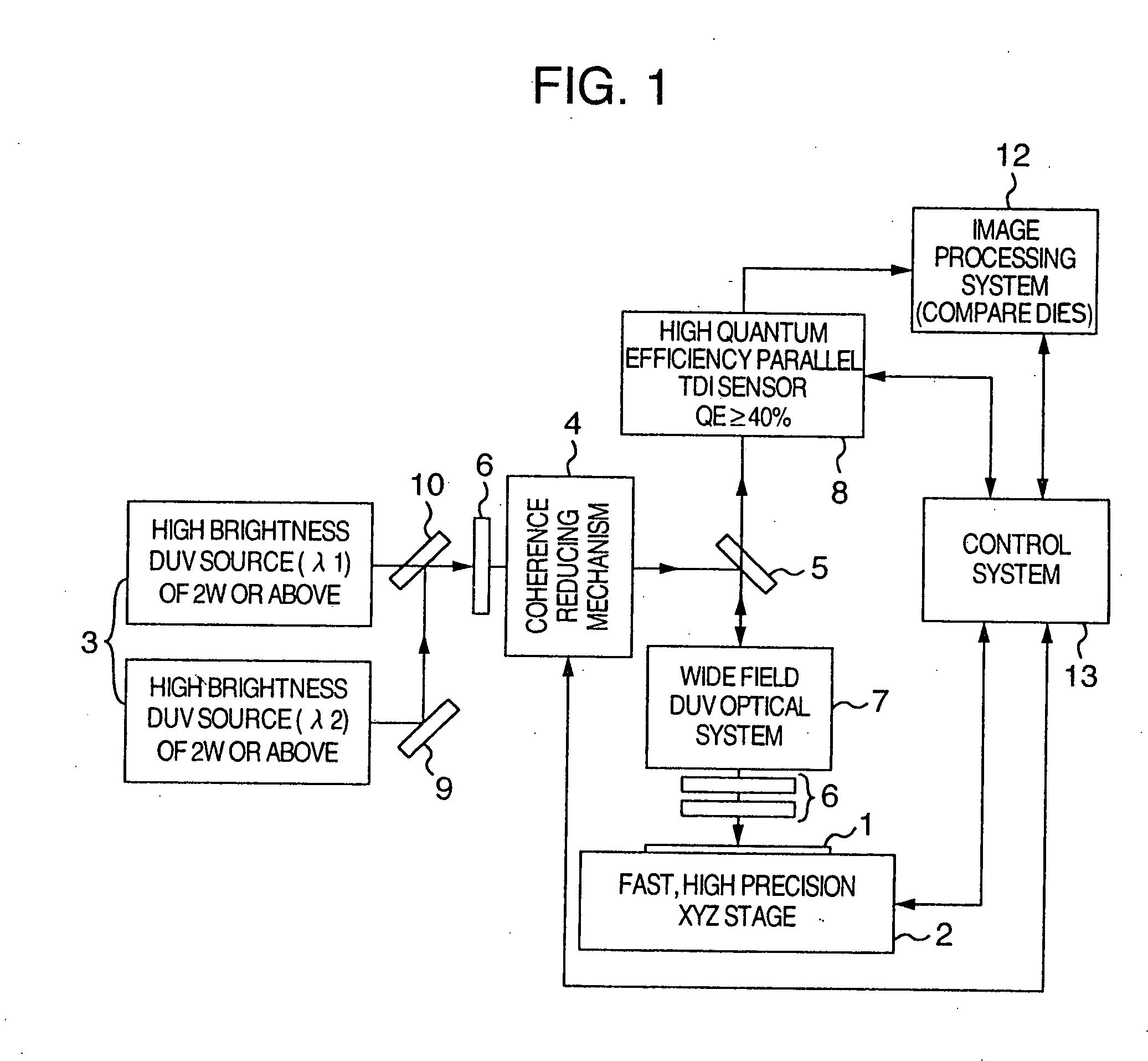
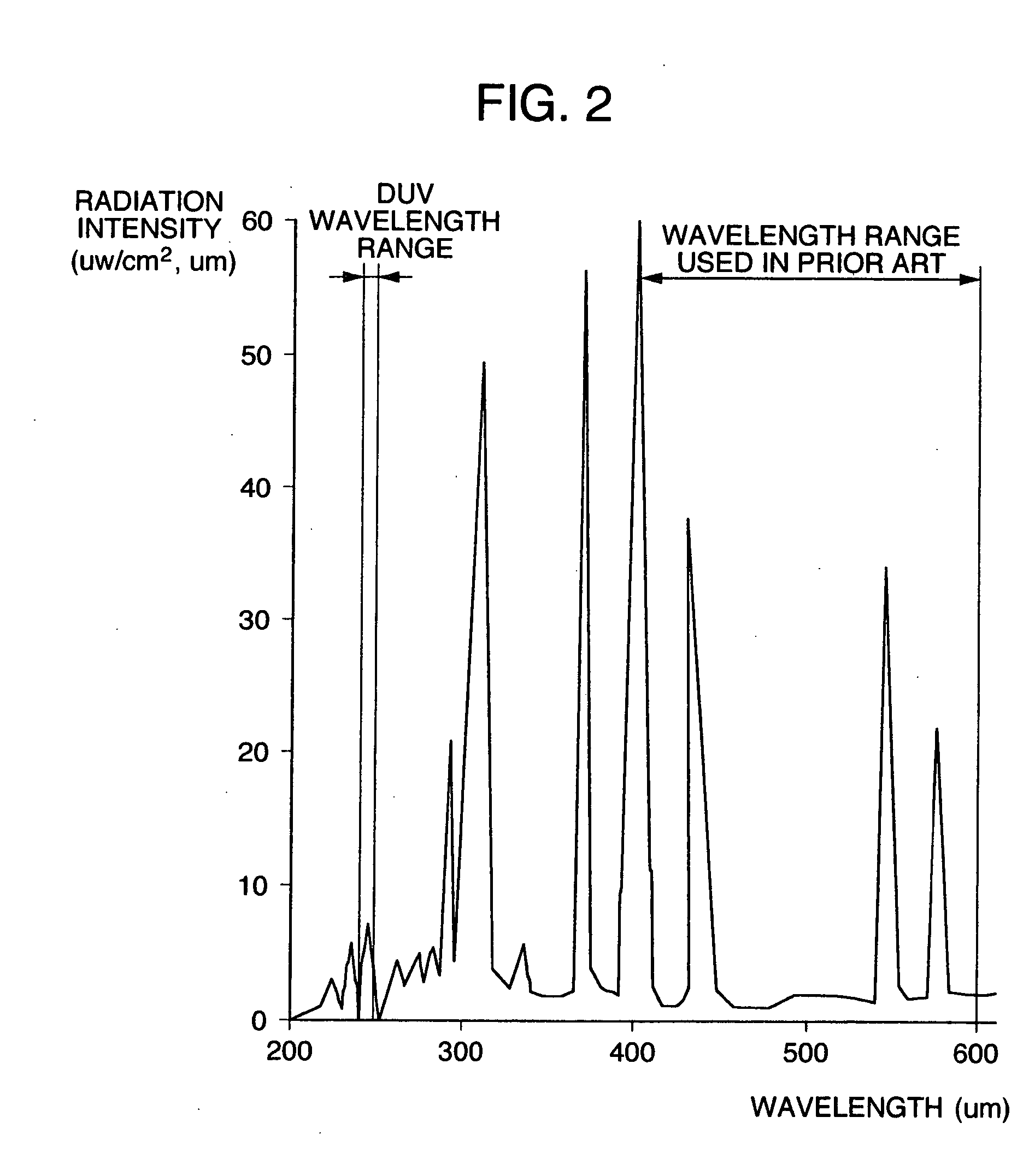
[0046] Embodiments of the defect inspection method and apparatus according to the invention will be described with reference to the accompanying drawings. FIG. 1 is a diagram showing one embodiment of the apparatus according to the invention. Referring to FIG. 1, there is shown an X, Y, Z, θ (rotation) stage 2 on which a semiconductor wafer 1 is placed as one example of the pattern being examined. There are also shown an optical system 7 including the objective lens, and illumination light source 3 (for example, UV laser sources of 266-nm wavelength and 257-nm wavelength) for illuminating the semiconductor waver 1. Here, while two laser sources are shown, a plurality of laser sources may be provided. In addition, the two wavelengths may be different or equal. These laser sources, when combined, generate various different effects. However, the optical system is corrected for wavelength according to the wavelength.

[0047] There is also shown a beam splitter (in some case, it may be a ...


PUM

PropertyMeasurementUnit
wavelengthaaaaaaaaaa
widthaaaaaaaaaa

Abstract

A defect inspection apparatus for inspecting a fine circuit pattern with high resolution to detect a defective portion is constructed to have an objective lens for detecting an image of a sample, a laser illumination unit for illuminating the sample through the objective lens, a unit for reducing the coherence of the laser illumination, an accumulation type detector, and a unit for processing the detected image signal.

Description

BACKGROUND OF THE INVENTION [0001] The present invention generally relates to pattern inspection and foreign substance inspection technology for detecting defects (such as short circuit and disconnection) and foreign objects on a pattern being examined, and particularly to a defect inspection method for examining defects and foreign objects on a pattern such as semiconductor wafer, liquid crystal display and photomask, and to a defect inspection apparatus using that method. In the following description, it is assumed that the defect includes a foreign object. [0002] There is known an inspection apparatus of this kind. As disclosed in JP-A-7-318326 (prior art 1), while a pattern to be examined is being moved, an imager such as line sensor is used to detect the image of the pattern, and the detected image signal and an image signal a certain time delayed from that signal are compared in their brightness so that a disagreement therebetween can be recognized as a defect. In addition, an...

Claims


Application Information

Patent Timeline
Patent Type & Authority Applications(United States)
IPC IPC(8): G01N21/956G01B11/30G02B21/06G06T1/00
CPCG01N21/956
Inventor MAEDA, SHUNJIYOSHIDA, ATSUSHISHIBATA, YUKIHIROYOSHIDA, MINORUUTO, SACHIOSHISHIDO, HIROAKINAKATA, TOSHIHIKO
Owner HITACHI LTD
Why Eureka
Try Eureka