Opto-electronic device and pulse processing method

a pulse processing and optoelectronic technology, applied in the field of optoelectronic devices, can solve the problems of complex optical and electrical setup, inability to process signals above frequencies in the upper thz range and up to phz range, and disadvantages of conventional stabilization laser sources based on the above approaches, so as to avoid disadvantages of conventional techniques , avoid disadvantages of conventional techniques

Active Publication Date: 2015-05-14
MAX PLANCK GESELLSCHAFT ZUR FOERDERUNG DER WISSENSCHAFTEN EV
View PDF5 Cites 11 Cited by
  • Summary
  • Abstract
  • Description
  • Claims
  • Application Information

AI Technical Summary

Benefits of technology

[0033]It is an objective of the present invention to provide an improved opto-electronic device for processing optical and electric pulses, being capable of avoiding disadvantages of conventional techniques. In particular, the opto-electronic device is to be capable of fully characterizing electric fields oscillating at light frequencies. For example, in the case of few cycle optical fields, the invention is to be capable of determining the absolute CE phase with a compact and reliable set-up. According to another particular aspect, the opto-electronic device is to be capable of outputting electric signals which are the result of ultrafast processing of information encoded in optical input signals. Such processing is to be performed with near- and beyond-petahertz (PHz) bandwidths. Furthermore, it is an objective of the present invention to provide an improved pulse processing method for processing ultra-short optical and electric pulses, being capable of avoiding disadvantages of conventional techniques.
[0041]According to a second aspect of the invention, a laser source device is provided which comprises a pulse source device being configured for creating ultra-short driving laser pulses and the opto-electronic device according to the above first aspect of the invention. According to the invention, the laser source device further comprises a control loop being capable of controlling the pulse source device in dependency on the electric output signal of the signal processing device. For example, the absolute CE phase of a laser pulse of the pulse train can be retrieved by measuring the photo-induced electric output signal. The feedback loop can subsequently act on the parameters of the laser source such as to minimize variations of the CE phase, e.g., act on the intensity of the pump laser of a titanium-sapphire (Ti:Sapph) oscillator, but not limited to that.
[0047]According to a further advantage, implementation of the present invention is not restricted to a particular band gap material. Multiple band gap materials are available, which preferably have a band gap energy Eg larger than the thermal energy available at the operation temperature of the optoelectronic device, in particular a minimum band gap energy of at least 1 meV. Thus, the charge carriers in the band gap material can be created exclusively by the influence of the driving laser pulses or alternatively exclusively by the field effect of injection laser pulses mentioned below. As preferred examples, the band gap material may comprise a semiconductor or insulator material, e. g., GaN, GaAs, Si, sapphire, SiO2 or diamond. These materials have additional advantages in terms of thermal stability during irradiation with the ultra-short laser pulses.
[0048]According to a further preferred embodiment of the invention, the opto-electronic device can be provided with a cooling device. According to this embodiment, an operation temperature of the photoconductor device can be adjusted. Advantageously, this allows a stabilization of the band gap material temperature even during the irradiation with the ultra-short laser pulses, and a thermal excitation of the band gap material can be excluded. Furthermore, the operation temperature adjustment allows to use materials, which at room temperature would have a band gap energy below the above minimum band gap energy, i.e., smaller than the thermal energy available at room temperature.

Problems solved by technology

Conventional techniques for stabilizing laser sources based on the above approaches have essential disadvantages in terms of complexity and stability of the optical and electrical set-up.
However, the above frequencies in the upper THz range and up to PHz range are not available for signal processing.

Method used


Image

  • Opto-electronic device and pulse processing method
  • Opto-electronic device and pulse processing method
  • Opto-electronic device and pulse processing method

Examples


Embodiment Construction

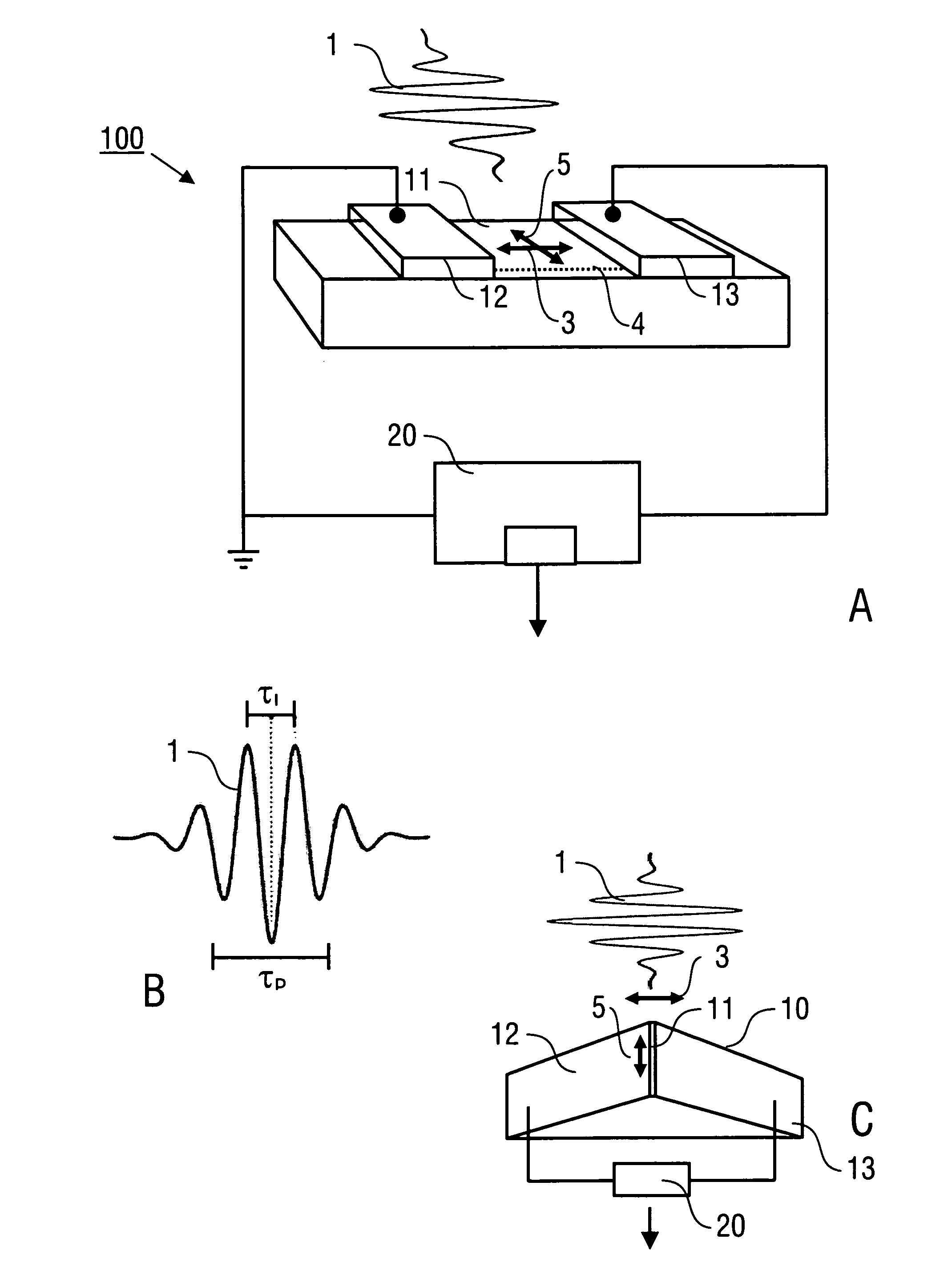
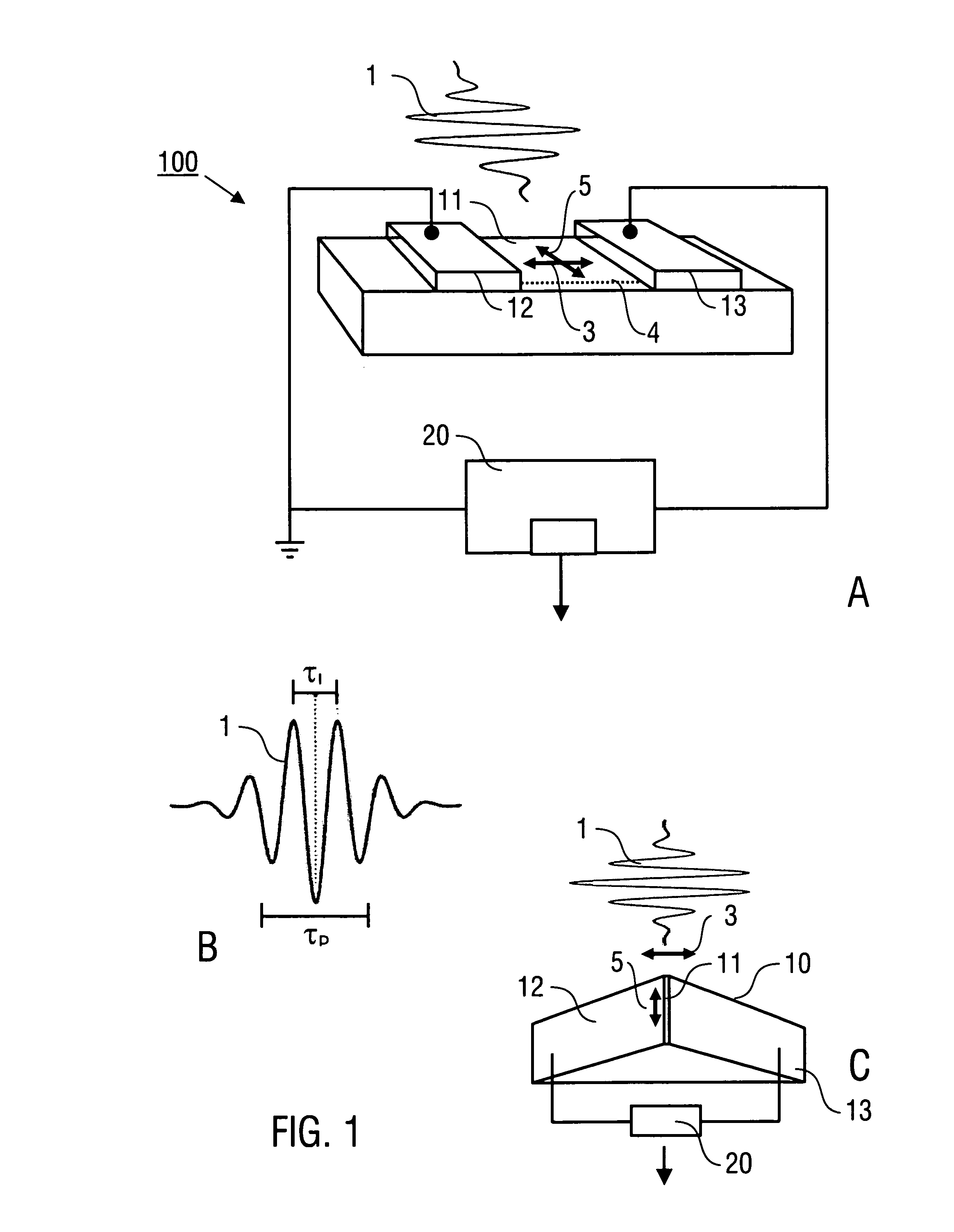
[0060]Embodiments of the invention are described in the following with exemplary reference to the figures which schematically show in particular the photoconductor device with electrical sensor contacts. It is emphasized that the implementation of the invention is not restricted to the illustrated embodiments, but is rather possible with other designs providing a sensor section exposed for an irradiation with laser pulses. In particular, the size and shape of the photoconductor device can be selected in dependency on the particular conditions of using the invention. Furthermore, the implementation of the invention is possible by integrating the optoelectronic device into an optical set-up as it is known from conventional pulse laser techniques.

[0061]FIG. 1A shows a first embodiment of an opto-electronic device 100 including a photoconductor device 10 with a sensor section 11 and electrical sensor contacts 12, 13 (collecting electrodes), and a signal processing device 20 which is con...


PUM


Abstract

An opto-electronic device (100) for processing optical and electric pulses includes a photoconductor device (10) with a sensor section (11) which is made of a band gap material and which has electrical sensor contacts (12, 13), and a signal processing device (20) which is connected with the sensor contacts (12, 13), wherein the photoconductor device (10) is adapted to create a photocurrent between the sensor contacts (12, 13) in response to an irradiation with ultra-short driving laser pulses (1) having a photon energy smaller than the energy band gap of the band gap material, having a non-zero electric field component (3) oriented parallel with a line (4) between the electrical sensor contacts (12, 13), and causing a charge carrier displacement in the band gap material, and wherein the signal processing device (20) is configured for an output of an electric signal being characteristic for at least one of carrier-envelope phase (CE phase), intensity, temporal properties, spectral intensity and spectral phase of the driving laser pulses (1). Furthermore, a laser source device including the opto-electronic device and pulse processing method for processing optical and electric pulses are described.

Description

TECHNICAL FIELD[0001]The present invention relates to an opto-electronic device, being adapted for processing optical and electric pulses, in particular to an opto-electronic device being capable of fully diagnosing electric fields oscillating at optical frequencies (e.g. measuring the carrier-envelope phase of ultra-short laser pulses) and / or creating electric outputs resulting from the ultrafast processing of information encoded in electromagnetic fields with optical bandwidths. Furthermore, the present invention relates to a pulse processing method for processing ultra-short optical and electric pulses. Applications of the invention are available in the fields of operating and diagnosing (in particular stabilizing) laser sources, and / or electric signal processing.TECHNICAL BACKGROUND OF THE INVENTION[0002]In the present specification, reference is made to the following publications cited for illustrating prior art techniques and conventional implementations of certain procedural ...

Claims


Application Information

Patent Timeline
Patent Type & Authority Applications(United States)
IPC IPC(8): H01S3/10G01J11/00
CPCG01J11/00H01S3/10H01L31/03044H01L31/09H01L31/0328Y02E10/544
Inventor SCHIFFRIN, AGUSTINERNSTORFER, RALPHKRAUSZ, FERENCPAASCH-COLBERG, TIM
Owner MAX PLANCK GESELLSCHAFT ZUR FOERDERUNG DER WISSENSCHAFTEN EV
Why Eureka
Try Eureka