Method and Apparatus for Detection and Identification of Counterfeit and Substandard Electronics

a technology of counterfeit electronic devices and methods, applied in the direction of flaw detection using microwaves, resistance/reactance/impedence, instruments, etc., can solve the problems of affecting the performance of devices and systems that use counterfeit electronic devices, semiconductor components, and many malfunctions of semiconductor components

Active Publication Date: 2015-05-21
NOKOMIS
View PDF3 Cites 29 Cited by
  • Summary
  • Abstract
  • Description
  • Claims
  • Application Information

AI Technical Summary

Benefits of technology

[0020]Yet another object of the present invention is to provide an apparatus for detection and / or identification of counterfeit and / or substandard electronic devices that energizes only power, clock and ground pins of such electronic devices.
[0047]A further object of the invention is to provide the sensor and integrated antenna enclosure that are configured into a single housing that is highly integrated that removes the need for interface connectors between the sensor assembly and the integrated antenna enclosure assembly.

Problems solved by technology

As is generally well known, counterfeit electronic devices, for example semiconductor components, are a wide-spread problem.
When installed in a fully functional product, the counterfeited semiconductor components often malfunction, fail due to environmental conditions, age prematurely, have unwanted functionality and in some cases just don't function at all despite a close electrical match, thus affecting performance of devices and systems that use them and inflicting financial losses due to inadequate performance.
Many of them are either superficial, extremely expensive or both superficial and extremely expensive.
Of superficial techniques, the simplest and most common is visual inspection, but as counterfeits have become increasingly sophisticated these techniques have become less reliable.
In contrast, more reliable techniques that can detect some counterfeiting modalities that are in existence are expensive or are destructive in nature.
During x-ray inspection the internal structure of like date and lot codes of electronic components are examined and compared to known authentic parts and certain types of counterfeit parts can be discovered, but these techniques are limited to physical external differences in the die, wirebonding etc.
Again, these techniques focus on the physical characteristics of the material that can be inspected when de-encapsulated and does not provide information regarding the underlying electronic functionality.
These techniques are also destructive in nature.
Chemical etching techniques which use acid to expose a wafer or die packaged in plastics or resins can likewise expose the internal components for inspection, but are destructive in nature.
Mechanical techniques including sanding, cutting, cracking, or chipping the ceramic or metal to expose wafer or die for inspection are also used with some success, but again result in destruction of the part being inspected.
Electrical tests range from full electrical tests, which are typically expensive, to gross leak and fine lead functional electrical testing.
One challenge is the need to collect emissions content on the part in a manner that shields the measurement from the external environment.

Method used


Image

  • Method and Apparatus for Detection and Identification of Counterfeit and Substandard Electronics
  • Method and Apparatus for Detection and Identification of Counterfeit and Substandard Electronics
  • Method and Apparatus for Detection and Identification of Counterfeit and Substandard Electronics

Examples


Embodiment Construction

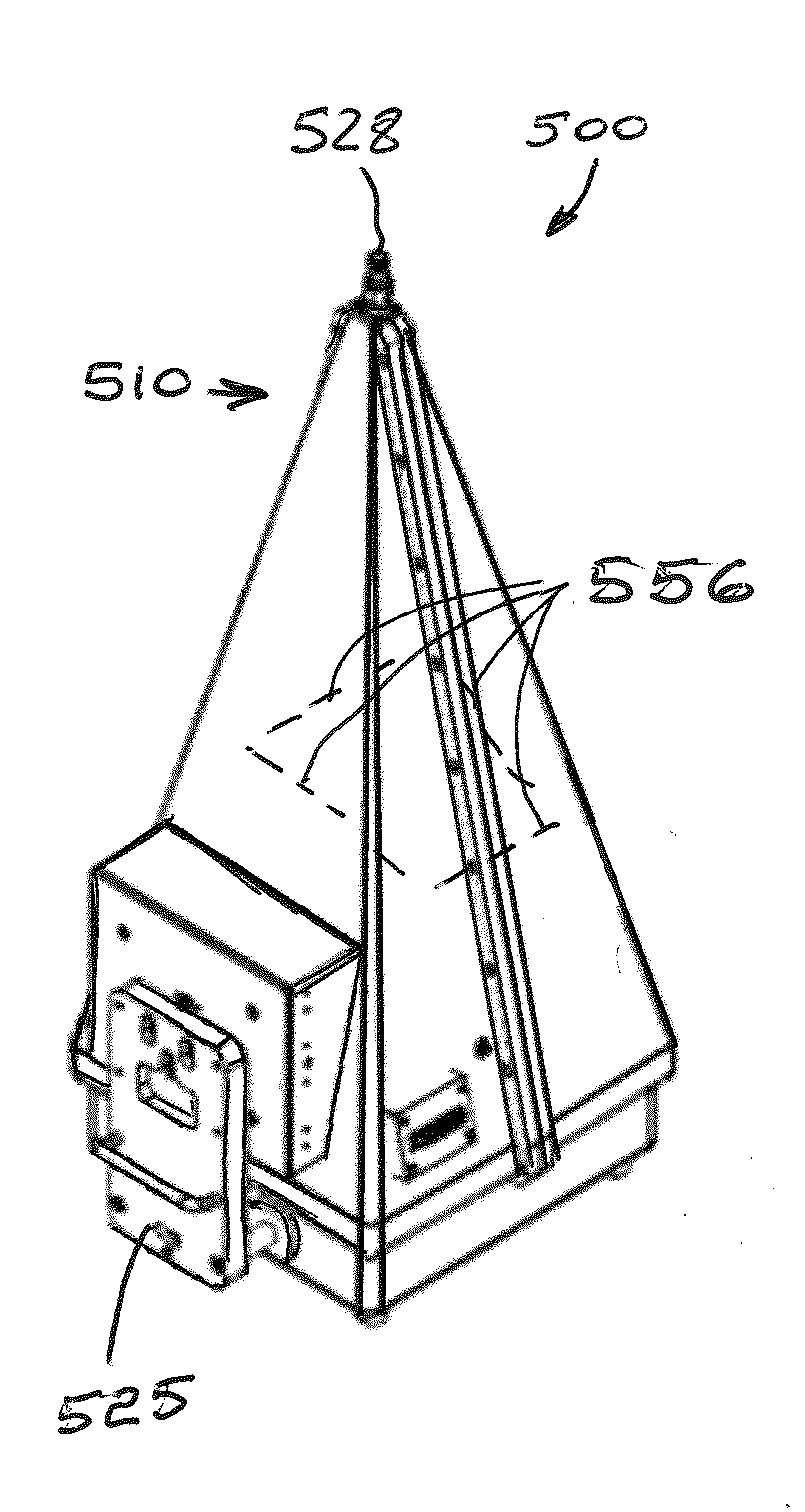
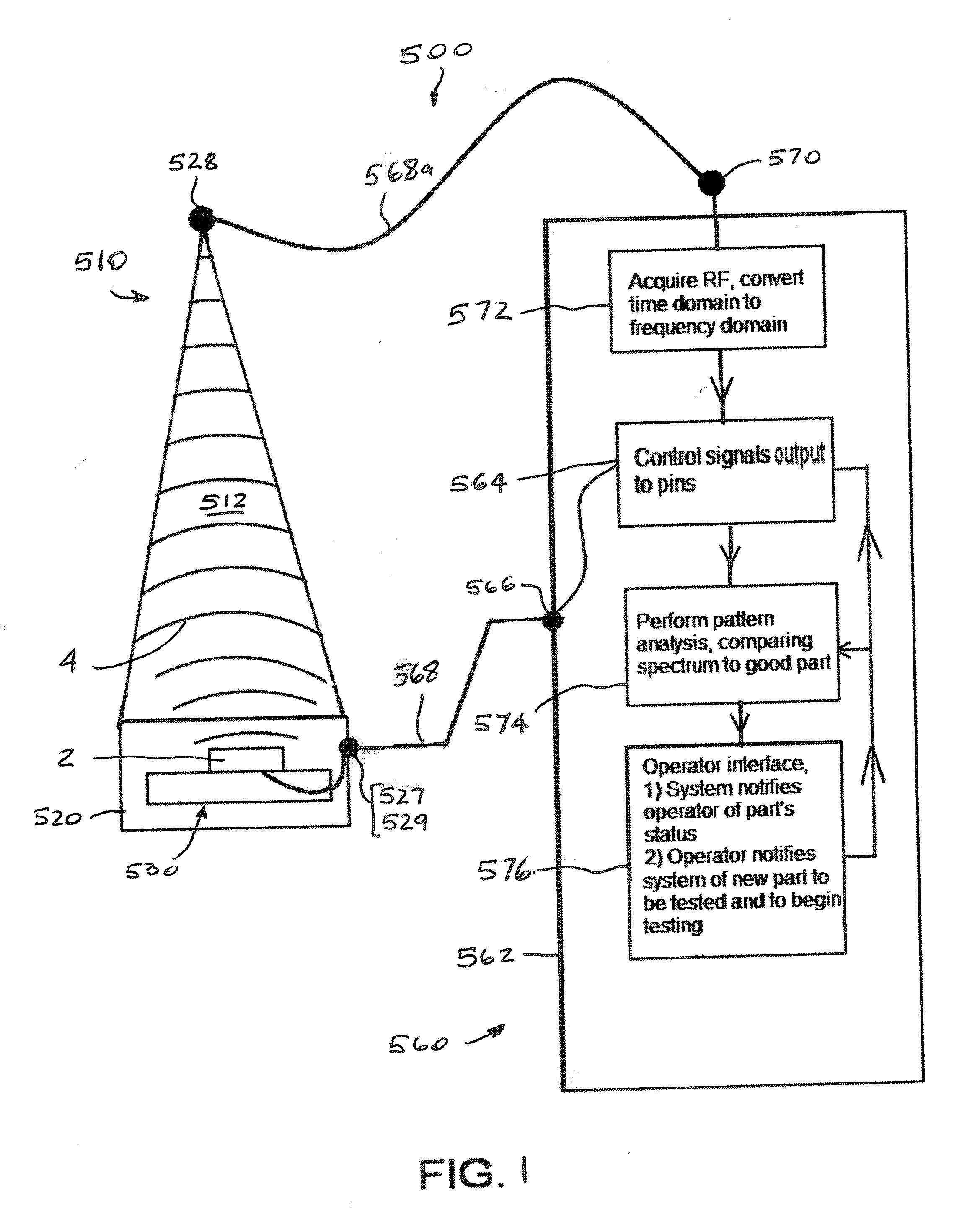
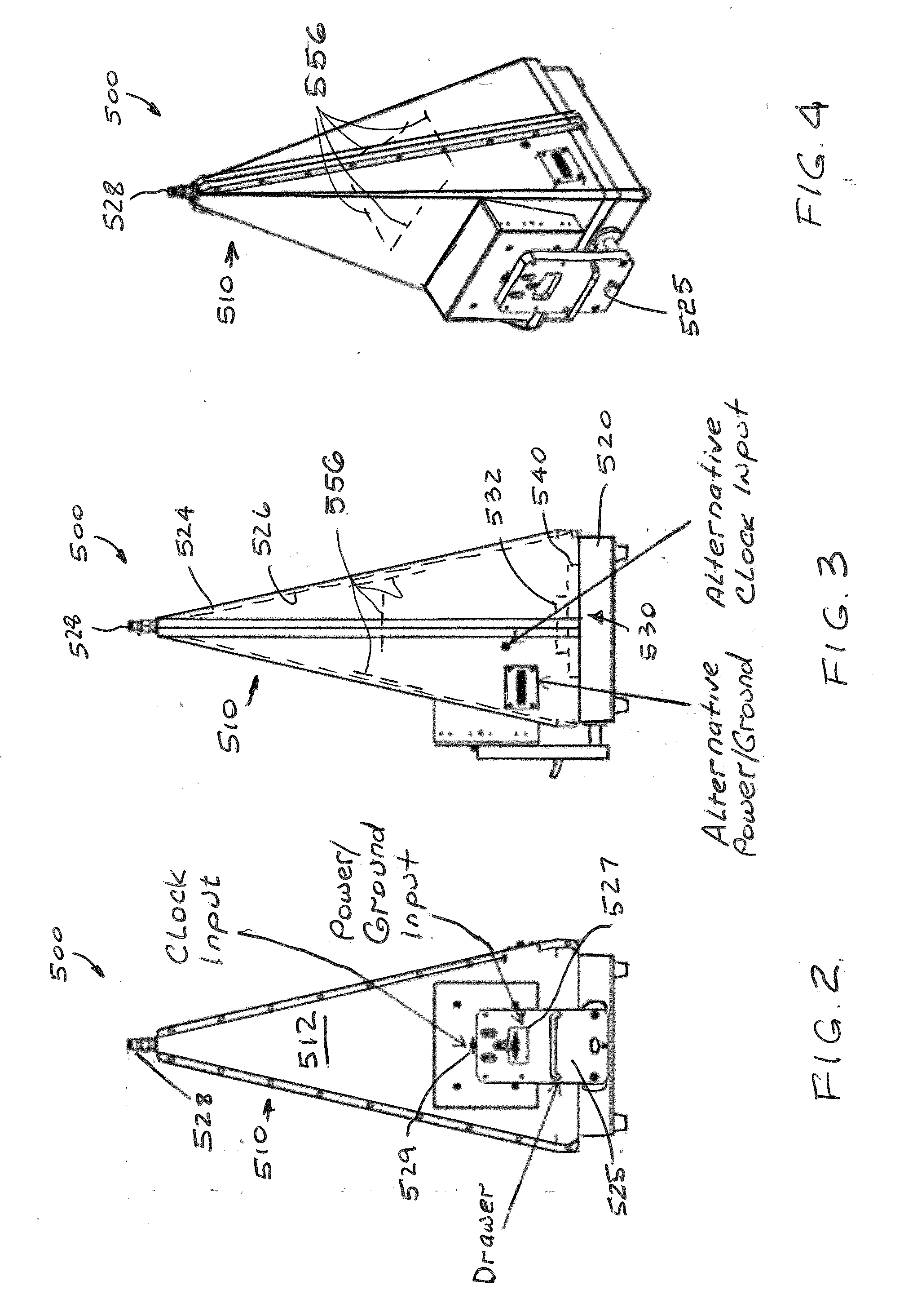
[0072]Prior to proceeding to the more detailed description of the present invention, it should be noted that, for the sake of clarity and understanding, identical components which have identical functions have been identified with identical reference numerals throughout the several views illustrated in the drawing figures.

[0073]It is to be understood that the definition of a counterfeit or substandard electronic device applies to but is not limited to work-alike electronic device, used electronic devices which have been removed from existing assemblies and sold as new and genuine parts, electronic devices which have been remarked to misrepresent their model / part number, manufacturer, cage code, date and / or lot code, reliability level, inspection, level of testing, or performance specification, electronic devices which do not conform to Original Component Manufacturer design, model, and / or performance standards, electronic devices which have been deliberately or unintentionally modif...


PUM

PropertyMeasurementUnit
thicknessaaaaaaaaaa
RF energyaaaaaaaaaa
phaseaaaaaaaaaa

Abstract

An apparatus for detecting a condition or authenticity of one or more electronic devices includes an enclosure having an antenna integrated therewithin, a fixture mounted within a hollow interior of the enclosure, the fixture being configured to receive the one or more electronic devices and connect one or more signals to each of the one or more electronic devices and a sensor and controller assembly connected to the antenna and configured to process a signature of an emission of a radiofrequency (RF) energy from of one or more electronic devices having the one or more signals connected thereto.

Description

CROSS-REFERENCE TO RELATED APPLICATIONS[0001]This application is related to and claims priority from U.S. Provisional Patent Application Ser. No. 61 / 851,323 filed on Mar. 6, 2013. This application is closely related to U.S. Ser. No. 13 / 410,797 filed on Mar. 2, 2012, entitled “SYSTEM AND METHOD FOR PHYSICALLY DETECTING COUNTERFEIT ELECTRONICS”, now published as US 2012-0226463 A1 and U.S. Ser. No. 13 / 410,909 filed on Mar. 2, 2012, entitled “INTEGRATED CIRCUIT WITH ELECTROMAGNETIC ENERGY ANOMALY DETECTION AND PROCESSING”, now published as US 2012-0223403 A1. These applications are being assigned to the assignee of the present invention and the disclosures of these applications are hereby incorporated by reference thereto.STATEMENT REGARDING FEDERALLY SPONSORED RESEARCH AND DEVELOPMENT[0002]This invention was made with government support under Small Business Innovative Research (SBIR) Contract N00024-12-C-4516 titled “Advanced Detection of Electronic Counterfeits” and awarded by the Un...

Claims


Application Information

Patent Timeline
Patent Type & Authority Applications(United States)
IPC IPC(8): G01N22/00G01N22/02
CPCG01N22/02G01N22/00H01L2924/0002G06F21/73G01R31/002Y04S40/20H01L2924/00
Inventor KELLER, III, WALTER JOHNPORTUNE, ANDREW RICHARDCHORNENKY, TODD ERICDAVIS, WILLIAM ANTHONY
Owner NOKOMIS
Why Eureka
Try Eureka