Semiconductor device

a semiconductor chip and semiconductor technology, applied in the field of power semiconductor devices, can solve the problems of difficulty in making internal repairs in the device, the need to replace the entire device, and the price of a semiconductor chip, so as to reduce the size of the device, reduce the cost and the number of components.

Active Publication Date: 2015-05-21
MITSUBISHI ELECTRIC CORP
View PDF7 Cites 13 Cited by
  • Summary
  • Abstract
  • Description
  • Claims
  • Application Information

AI Technical Summary

Benefits of technology

[0007]The present invention makes it possible to reduce the cost and...

Problems solved by technology

When even only one of the semiconductor chips is broken, a need arises to replace the entire device because it is difficult to make internal repairs in the device.
The unit pri...

Method used


Image

  • Semiconductor device
  • Semiconductor device
  • Semiconductor device

Examples


embodiment 1

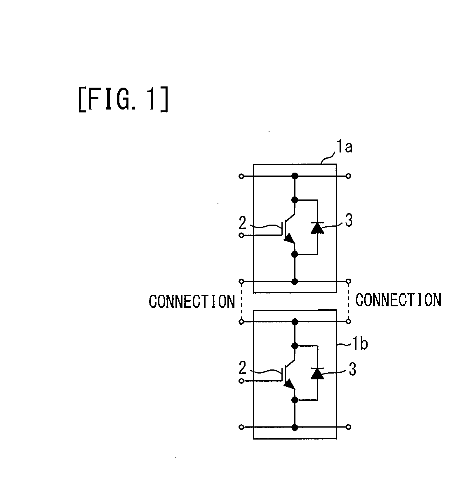
[0023]FIG. 1 is a circuit diagram showing a semiconductor device according to Embodiment 1 of the present invention. Two semiconductor modules 1a and 1b are connected in series to each other. Each of the semiconductor modules 1a and 1b has an IGBT 2 (Insulated Gate Bipolar Transistor) 2 and an FWD 3 (Free Wheeling Diode) connected in parallel with each other.

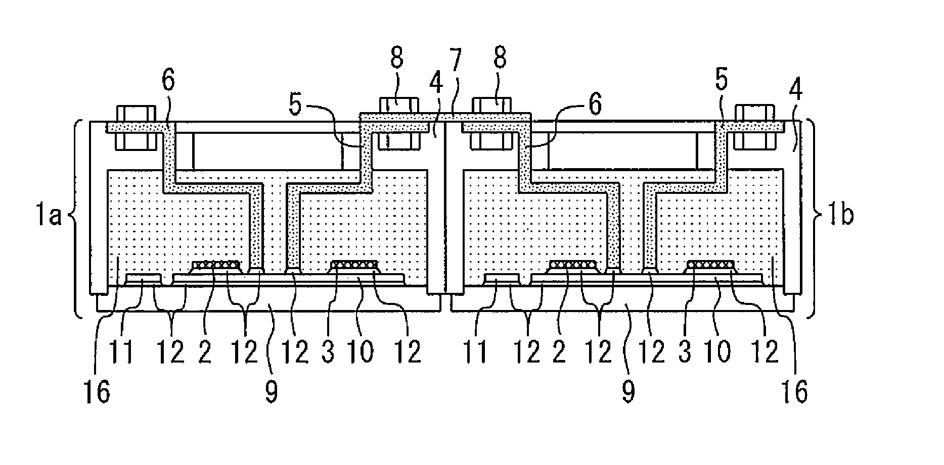
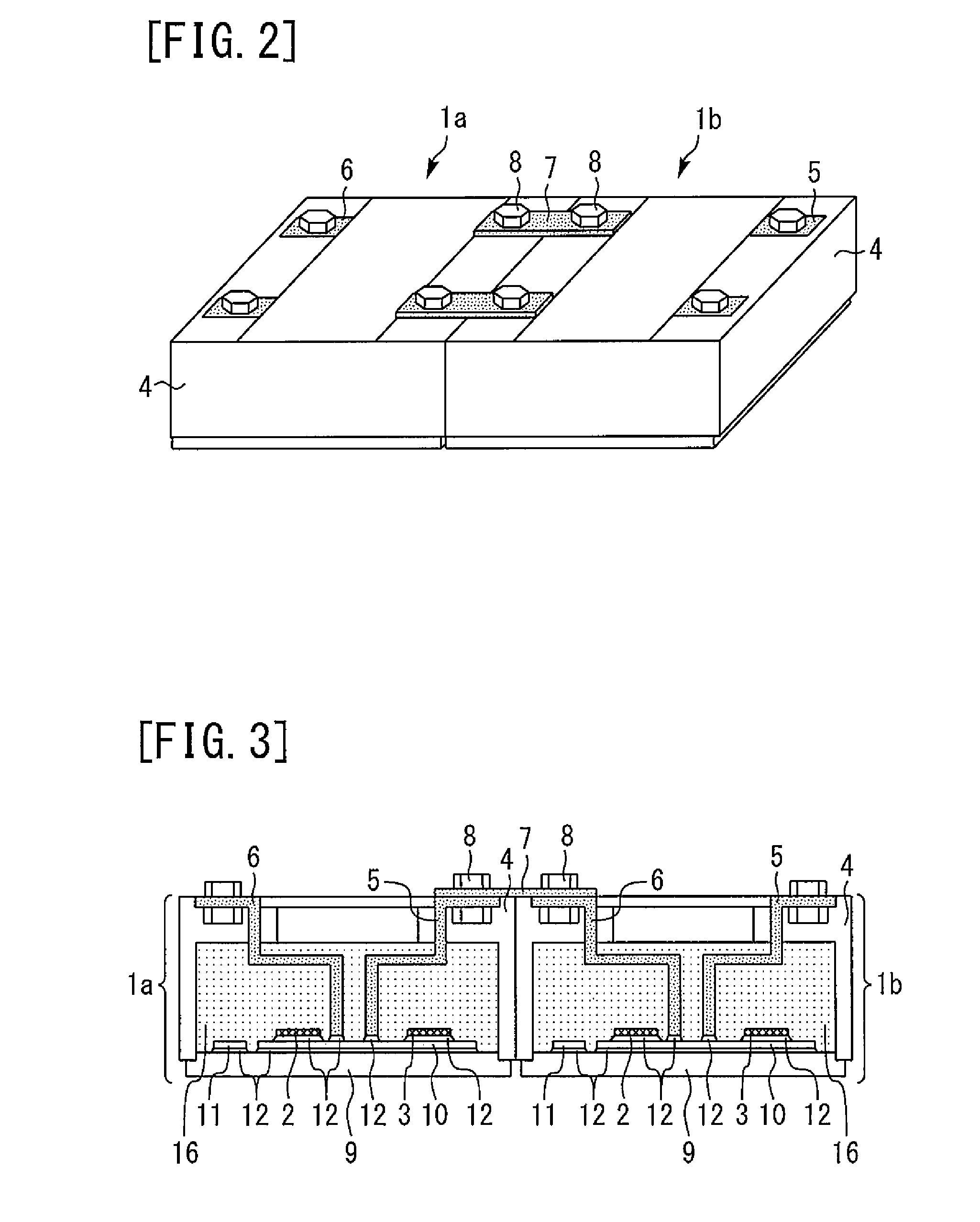
[0024]FIG. 2 is a perspective view showing the semiconductor device according to Embodiment 1 of the present invention. A collector main electrode 5 and an emitter main electrode 6 of the semiconductor modules 1a and 1b are led out to upper surfaces of cases 4. The collector main electrode 5 and the emitter main electrode 6 are connected to an external circuit or an adjacent semiconductor module. A connecting electrode 7 formed only of an electrically conductive plate made of Al or Cu is connected and fixed to another collector main electrode 5 of the semiconductor module 1a and another emitter main electrode 6 of the semiconduc...

embodiment 2

[0032]FIG. 8 is a sectional view showing a semiconductor device according to Embodiment 2 of the present invention. The connecting electrode 7 is bent downward at its opposite ends to form hook portions 17. Grooves 18 in which the hook portions 17 can be caught are provided in the upper surfaces of the cases 4 of the semiconductor modules 1a and 1b, thereby facilitating positioning of the semiconductor modules 1a and 1b relative to each other.

embodiment 3

[0033]FIG. 9 is a sectional view showing a semiconductor device according to Embodiment 3 of the present invention. Recesses 19 are provided in the upper surfaces of the cases 4. The collector main electrode 5 and the emitter main electrode 6 are led out to bottom surfaces of the recesses 19. In the recesses 19, the connecting electrode 7 is connected and fixed to the collector main electrode 5 and the emitter main electrode 6. The position at which the bolts 8 are mounted on the collector main electrode 5 and the emitter main electrode 6 is thus lowered. A certain insulation distance to an external device connected adjacent to the semiconductor device can thereby be secured, thus improving the insulation performance.


PUM


Abstract

Each of semiconductor module includes a semiconductor chip, a case surrounding the semiconductor chip, and a main electrode connected to the semiconductor chip and led out to an upper surface of case. A connecting electrode is connected and fixed to the main electrodes of the adjacent semiconductor modules. The connecting electrode is formed only of a metal plate. The rated current, the rated voltage and the circuit configuration can easily be changed by changing the connection using the connecting electrode, thus enabling reduction of the design time and facilitating manufacture management. Only a malfunctioning one of the semiconductor modules may be replaced. There is, therefore, no need to replace the entire device. The connecting electrode is formed of an electrically conductive plate and, therefore, enables reduction of the number of component parts and reduction of the device in size in comparison with the conventional wiring bus bar.

Description

TECHNICAL FIELD[0001]The present invention relates to a power semiconductor device used for motor control, for example, in electric railway use, on industrial equipment, or on consumer equipment.BACKGROUND ART[0002]It is necessary for semiconductor manufacturers to determine, for example, a rated current, a rated voltage and a circuit configuration in designing a semiconductor device according to use of the semiconductor device and to provide parts and perform manufacture management according to a lineup of various semiconductor devices. Simultaneously, users are required to make preparations for and management of semiconductor devices for pieces of equipment. A semiconductor device has a number of semiconductor chips mounted therein. When even only one of the semiconductor chips is broken, a need arises to replace the entire device because it is difficult to make internal repairs in the device. The unit price of a semiconductor chip using SiC in particular is higher than that of an...

Claims


Application Information

Patent Timeline
IPC IPC(8): H05K7/02H01L23/04H01L25/10
CPCH05K7/02H01L23/04H01L25/105H01L25/18H01L2224/32225H01L2224/48227H01L2224/49175H01L2224/73265H05K1/0263H01L23/3735H01L23/49811H01L23/49838H01L2924/30107H01L2924/13091H01L25/115H01L2924/13055H01L2924/1305H01L23/24H01L24/73H01L2224/0603H01L2224/49111H01L2224/49113H01L2924/00012H01L2924/00
Inventor TSUDA, RYOMORISHITA, KAZUHIRO
Owner MITSUBISHI ELECTRIC CORP
Why Eureka
Try Eureka