Solar cell and method of manufacturing the same

a solar cell and back contact technology, applied in the field of solar cells, can solve the problems of low efficiency of solar cells, and achieve the effects of maximizing photoelectric conversion, easy adjustment, and increasing the size of the first conductive type region

Active Publication Date: 2015-05-28
SHANGRAO JINKO SOLAR TECH DEV CO LTD
View PDF4 Cites 57 Cited by
  • Summary
  • Abstract
  • Description
  • Claims
  • Application Information

AI Technical Summary

Benefits of technology

[0007]Embodiments of the invention provide a solar cell having enhanced efficiency and a method of manufacturing the same.
[0028]In the embodiments of the invention, a conductive type region includes a boundary region and thus the area of the conductive type region participating in photoelectric conversion may be maximized. In this regard, the size of the first conductive type region functioning as an emitter region may further be increased by forming a width of a boundary region of the first conductive type region having a conductive type opposite that of the base region to be greater than a width of a boundary region of the second conductive type region having the same conductive type as that of the base region. In this regard, when the first conductive type region is of a p-type and the second conductive type region is of an n-type, the widths of the boundary regions of the first and second conductive type regions may be easily adjusted using properties of first and second conductive type impurities without further performing separate manufacturing processes or further using separate devices. As such, the areas of the first and second conductive type regions are maximized and, in particular, the size of the first conductive type region is further increased and, accordingly, efficiency of the solar cell may be enhanced.
[0029]The first and second conductive type regions may be easily formed by ion implantation and the widths thereof may also be easily adjusted. According to the manufacturing method according to the embodiment of the invention, a solar cell having an improved structure may be manufactured using simplified and easy manufacturing processes.

Problems solved by technology

For widespread use of the solar cells, low efficiency thereof needs to be overcome.

Method used


Image

  • Solar cell and method of manufacturing the same
  • Solar cell and method of manufacturing the same
  • Solar cell and method of manufacturing the same

Examples


Embodiment Construction

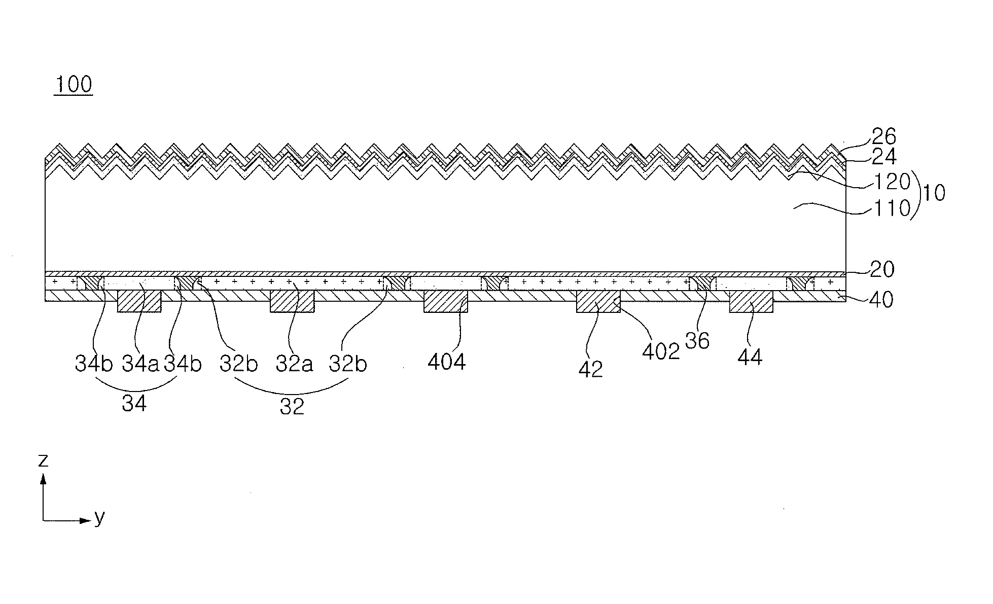
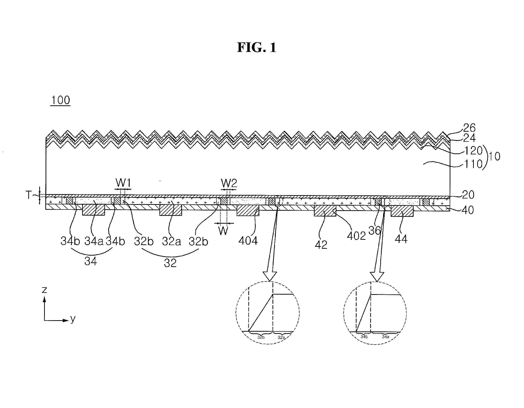
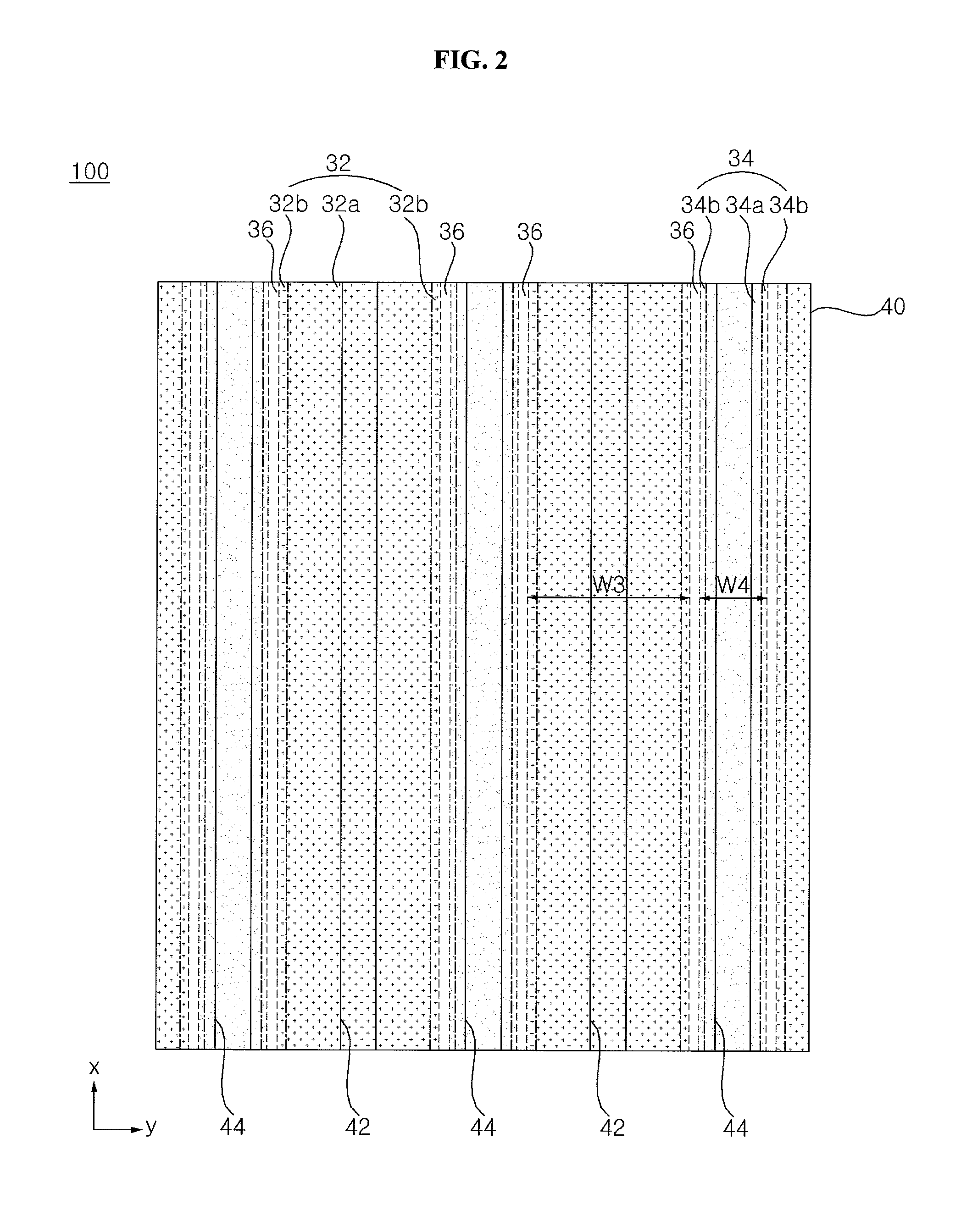
[0041]Reference will now be made in detail to embodiments of the invention, examples of which are illustrated in the accompanying drawings. However, the invention may be embodied in many different forms and should not be construed as limited to the embodiments set forth herein.

[0042]Only elements constituting features of the embodiments of the invention are illustrated in the accompanying drawings and other elements that will not be described herein are omitted from the drawings, for clarity of description. Like reference numerals refer to like elements throughout. In the drawings, the thicknesses, areas, etc., of constituent elements may be exaggerated or reduced for clarity and convenience of illustration. The embodiments of the invention are not limited to the illustrated thicknesses, areas, etc.

[0043]It will be further understood that, throughout this specification, when one element is referred to as “comprising” another element, the term “comprising” specifies the presence of a...


PUM


Abstract

A solar cell is discussed. The solar cell according to an embodiment includes a semiconductor substrate, a first conductive type region and a second conductive type region disposed on the same side of the semiconductor substrate, wherein at least one of the first and second conductive type regions includes a main region and a boundary region disposed at a peripheral portion of the main region, and the boundary region has at least one of a varying doping concentration and a varying doping depth.

Description

CROSS-REFERENCE TO RELATED APPLICATION[0001]This application claims the priority benefit of Korean Patent Application No. 10-2013-0146519, filed on Nov. 28, 2013 in the Korean Intellectual Property Office, the disclosure of which is incorporated herein by reference.BACKGROUND OF THE INVENTION[0002]1. Field of the Invention[0003]Embodiments of the invention relate to a solar cell and a method of manufacturing the same, and more particularly to a back contact solar cell and a method of manufacturing the same.[0004]2. Description of the Related Art[0005]Recently, as existing energy resources such as petroleum and coal are running out, interest in alternative energy sources is increasing. In particular, solar cells, which directly convert solar energy into electric energy, are receiving much attention as a next-generation alternative energy source.[0006]These solar cells may be manufactured by forming various layers and electrodes according to a design. In this regard, efficiency of a s...

Claims


Application Information

Patent Timeline
Patent Type & Authority Applications(United States)
IPC IPC(8): H01L31/0352H01L31/18H01L31/0224
CPCH01L31/035272H01L31/1804H01L31/1864H01L31/022441H01L21/266H01L31/0747H01L31/03529Y02E10/547Y02P70/50
Inventor YANG, YOUNGSUNGCHOI, JUNGHOONPARK, HYUNJUNG
Owner SHANGRAO JINKO SOLAR TECH DEV CO LTD
Why Eureka
Try Eureka