Solar cell unit

a solar cell and unit technology, applied in the direction of diodes, semiconductor devices, electrical apparatus, etc., to achieve the effects of high temperature stability, good uv transparency, and strong frictional connection of secondary optical elements

Active Publication Date: 2015-05-28
AZUR SPACE SOLAR POWER
View PDF2 Cites 3 Cited by
  • Summary
  • Abstract
  • Description
  • Claims
  • Application Information

AI Technical Summary

Benefits of technology

[0016]In an embodiment, the substrate at least in one direction, preferably in both directions can be formed within the top side plane of the substrate, has a greater lateral extension than the secondary optical element. Experiments have shown that as a result according to a refinement the polymer adhesive layer projects laterally over the surface on the bottom side of the secondary optical element and an especially strong frictional connection of the secondary optical element with the substrate can be achieved.
[0017]In an embodiment, the secondary optical element can be configured in the shape of a half-ellipsoid and preferably has a circumferential shoulder-shaped collar. In a further embodiment, the secondary optical element is configured in the shape of a truncated pyramid or funnel. It is preferred, furthermore, to make the secondary optical element as a single piece of an inorganic material, preferably of a quartz glass compound. An advantage of the inorganic material or quartz glass compound is the very good UV transparency and the extraordinary high temperature stability and high mechanical and chemical resistance in comparison with an organic or plastic compound.
[0018]In another embodiment, a metal layer can be formed on the bottom side of the substrate as part of the substrate, whereby the metal layer is preferably not formed in a circumferential edge region directly at the edge of the substrate. An advantage of the metal layer is that compared with a substrate without a back metal layer, the heat is transferred from the top side of the substrate uniformly to the entire substrate. Experiments have shown that a higher radiation from the bottom side also occurs due to the more uniform distribution of heat. Further, when the substrate is mounted on a base, the heat transfer resistance between the base and the substrate is reduced by means of the back metal layer.

Problems solved by technology

Solar cell units of this type can be used in so-called CPV systems, among other things because of the higher manufacturing costs compared with silicon solar cells.

Method used


Image

  • Solar cell unit
  • Solar cell unit
  • Solar cell unit

Examples


Embodiment Construction

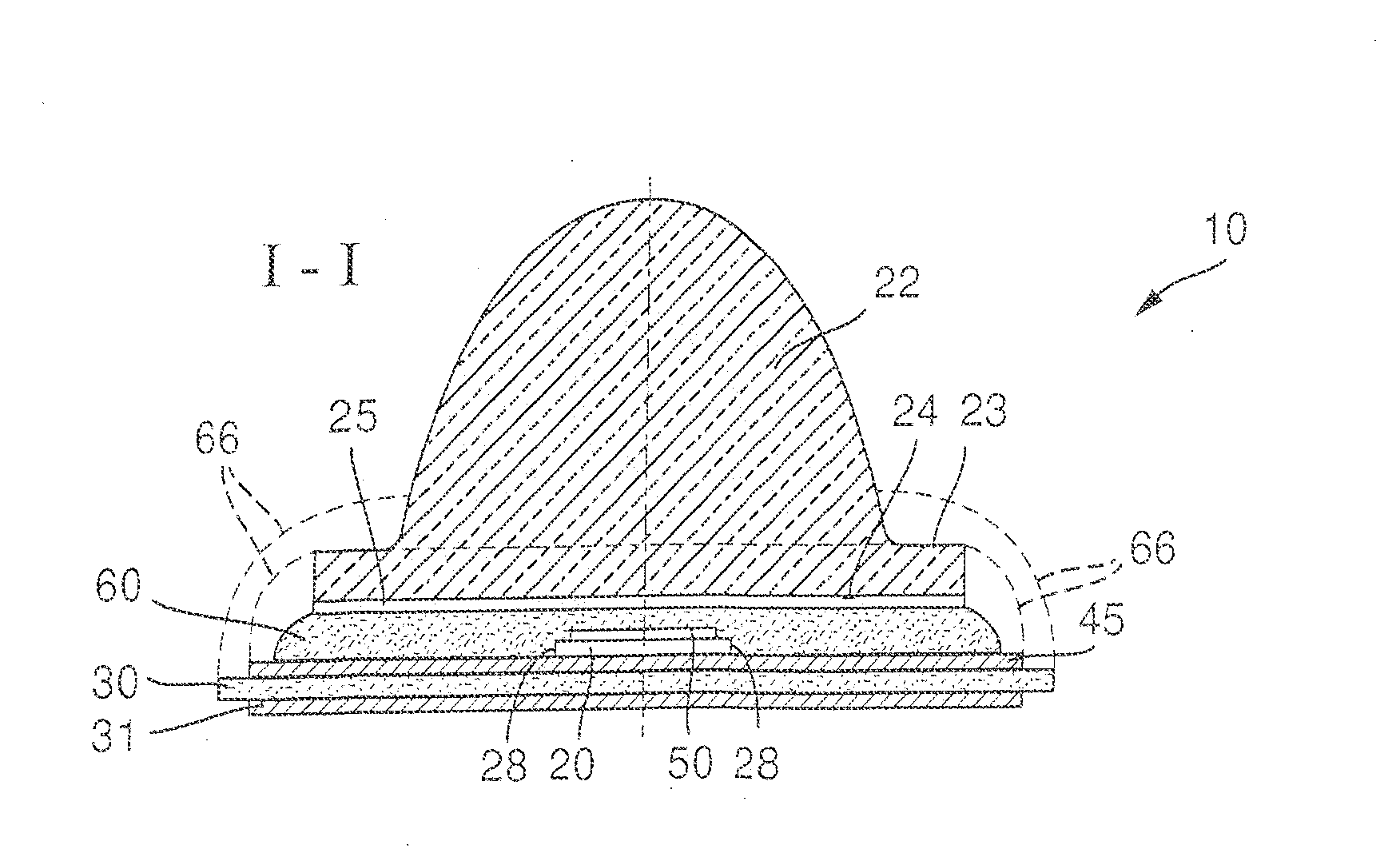
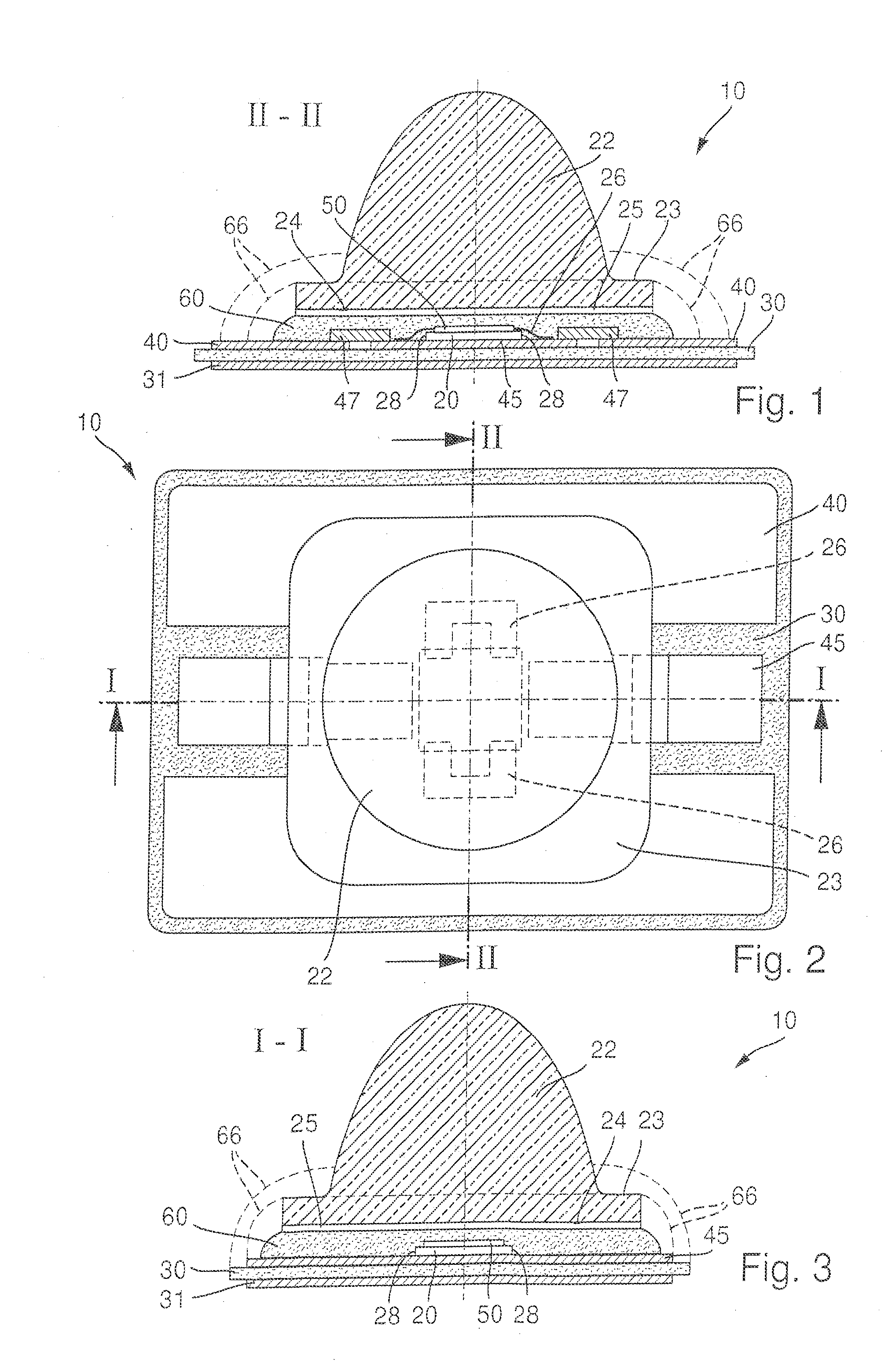
[0030]The illustration in FIG. 1 shows a solar cell unit 10 with a semiconductor body 20 formed as a solar cell, a secondary optical element 22 in the shape of a half-ellipsoid with a circumferential collar-shaped bead 23. Secondary optical element 22 has a bottom side 24 and guides the light incident on secondary optical element 22 to the front side of semiconductor body 20. Optical element 22 has a planar surface on the entire bottom side 24, whereby part of the planar surface is arranged above a front side of semiconductor body 20. A first adhesion-promoting layer 25 connected by material bonding to bottom side 24 is formed on the entire bottom side 24. Substrate 30 on the bottom side has a full-surface metal layer 31 except for a narrow edge region. Substrate 30 in addition has a greater lateral extension than secondary optical element 22.

[0031]Semiconductor body 20 furthermore has a front side with a first electrical connection and a back side with a second electrical connectio...


PUM


Abstract

A solar cell unit having a semiconductor body formed as a solar cell, whereby the semiconductor body has a front side with a first electrical connection and a back side with a second electrical connection and a side surface formed between the front side and the back side, and having a substrate with a top side and a bottom side, whereby the substrate on the top side has a first conductive trace region, configured as part of the substrate, and the first electrical connection is electrically connected to the first conductive trace region, and the substrate on the top side has a second conductive trace region, configured as part of the substrate, and the second electrical connection is electrically connected to the second conductive trace region, and having a secondary optical element, which has a bottom side and guides light to the front side of the semiconductor body.

Description

[0001]This nonprovisional application is a continuation of International Application No. PCT / EP2013 / 002168, which was filed on Jul. 22, 2013 and which claims priority to European Patent Application No. EP 12005554.6, which was filed on Jul. 31, 2012, and which is herein incorporated by reference.BACKGROUND OF THE INVENTION[0002]1. Field of the Invention[0003]The present invention relates to a solar cell unit.[0004]2. Description of the Background Art[0005]A solar cell module is known from EP 2 073 279 A1, which corresponds to US 2010 / 0132793, in which a semiconductor body formed as a solar cell is arranged on a substrate. In order to protect the semiconductor body and particularly the side surfaces thereof from environmental influences, which lead to a degradation of the electrical parameters, a frame is arranged on four sides around the semiconductor body and closed with a transparent cover. Next, the remaining interspace is filled with a transparent sealing compound and an optical...

Claims


Application Information

Patent Timeline
Patent Type & Authority Applications(United States)
IPC IPC(8): H01L31/0232H01L31/0203H01L27/142H01L31/02
CPCH01L31/02327H01L27/1421H01L31/0203H01L31/02008H01L31/048Y02E10/52H01L31/0543
Inventor KHORENKO, VICTORZRINSCAK, IVICA
Owner AZUR SPACE SOLAR POWER
Why Eureka
Try Eureka