
Organic light emitting diode display, and fabricating and inspecting methods thereof

a light-emitting diode and organic technology, applied in the field of organic light-emitting diode displays, can solve the problems of high probability of high-resolution displays, failure of the line connecting the source electrode of the driving thin film transistor drt and the anode electrode of the organic light-emitting diode el, corrosion, non-patterning or step difference failure, etc., to achieve the effect of reducing, through redundancy structure, and malfunction

Active Publication Date: 2015-06-11
LG DISPLAY CO LTD
View PDF3 Cites 6 Cited by
  • Summary
  • Abstract
  • Description
  • Claims
  • Application Information

AI Technical Summary

Benefits of technology

The present invention provides an organic light emitting diode display and a fabricating method that can minimize malfunctions caused by open failures due to a step difference in the fabricating process. It also provides an inspecting method that can easily detect and repair failures in a pixel structure where an additional open failure occurs. Additionally, at least one contact part is formed to ensure a normal application of signals even when an open failure occurs. It further describes a method for easily deciding the occurrence of an open failure by applying a voltage of predetermined potential.

Problems solved by technology

The high-resolution display has a high probability that a failure such as corrosion, non-patterning or step difference failure may occur in a fabrication process of the high-resolution display, as compared with the existing high-resolution displays.
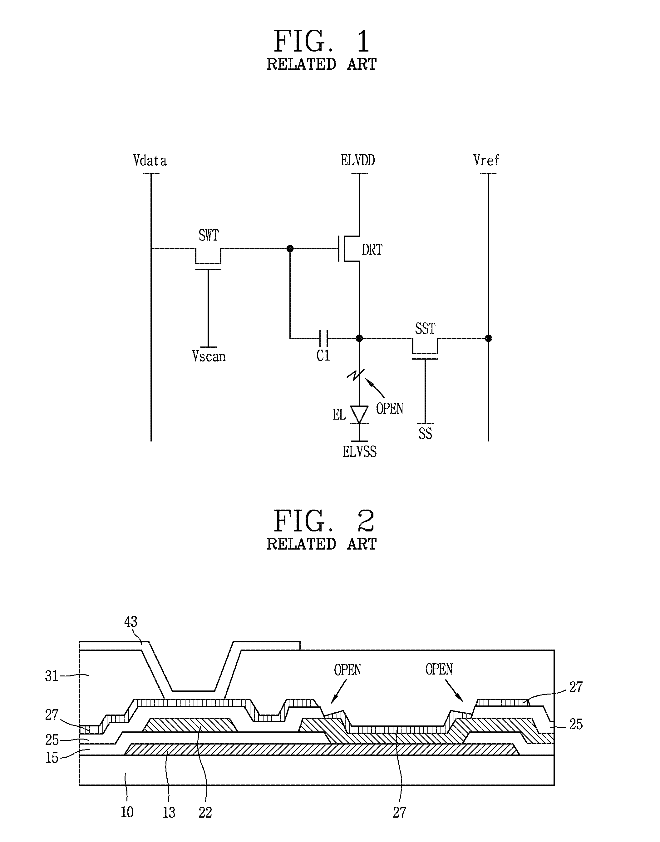
Particularly, in the OLED display having the pixel structure described above, there frequently occurs a failure that a line for connecting between the source electrode of the driving thin film transistor DRT and an anode electrode of the organic light emitting diode EL is opened.
The lines are formed in different metal layers to be contacted with each other, and the upper metal layer is over-etched in an etching process due to a step difference of the lower metal layer, thereby resulting in the failure.
This becomes a factor that causes an unexpected malfunction of the OLED display, thereby deteriorating the driving reliability of the display.

Method used


Image

  • Organic light emitting diode display, and fabricating and inspecting methods thereof
  • Organic light emitting diode display, and fabricating and inspecting methods thereof
  • Organic light emitting diode display, and fabricating and inspecting methods thereof

Examples


Embodiment Construction

[0032]Description will now be given in detail of the exemplary embodiments of the present invention, with reference to the accompanying drawings. For the sake of brief description with reference to the drawings, the same or equivalent components will be provided with the same reference numbers, and description thereof will not be repeated.

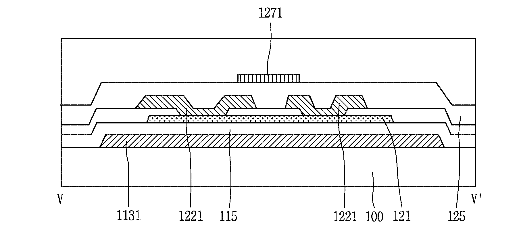
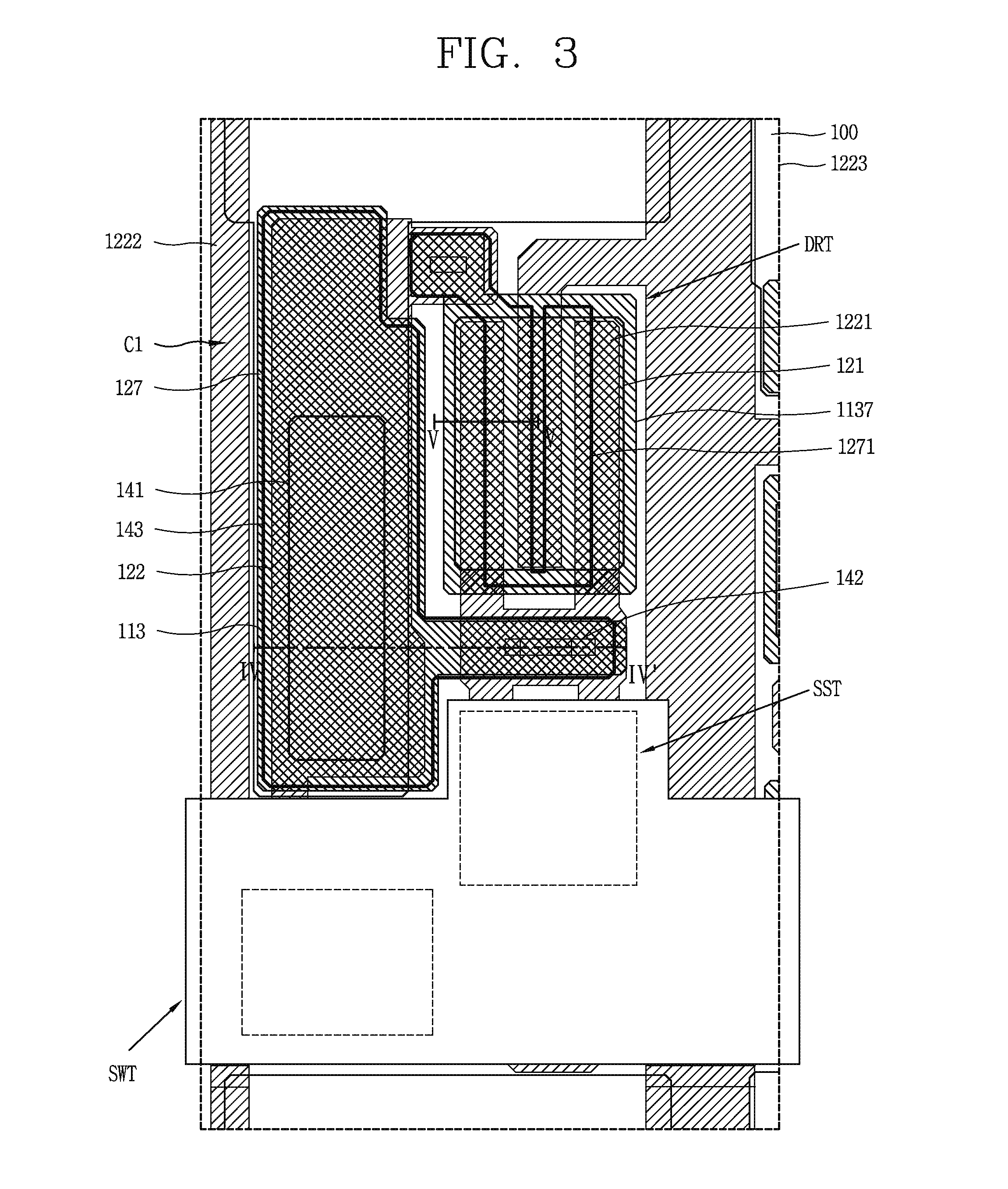
[0033]FIG. 3 is a plan view of a pixel of an organic light emitting diode display according to an exemplary embodiment of the present invention, and FIGS. 4A and 4B are section views respectively illustrating portions IV-IV′ and V-V′ of FIG. 3. The pixel of the organic light emitting diode display according to one or more embodiments of the present invention includes three thin film transistors.

[0034]Referring to FIGS. 3-4B, in the organic light emitting diode display according to the present disclosure, a gate metal layer 113 including a gate electrode and a signal line is formed on a substrate 100. Here, the substrate 100 may be made of a flexibl...


PUM


Abstract

Discussed are an organic light emitting diode display which can minimize a malfunction due to an open failure caused in a fabricating process of the organic light emitting diode display using thin film transistors as control elements, and fabricating and inspecting method of the organic light emitting diode display. Accordingly, at least one contact part is further formed by forming an upper metal layer of a dual gate structure with respect to an area in which an open failure easily occurs due to a step difference on a substrate of the organic light emitting diode display, so that a signal can be normally applied even when the open failure occurs.

Description

CROSS-REFERENCE TO RELATED APPLICATIONS[0001]Pursuant to 35 U.S.C. §119(a), this application claims the benefit of earlier filing date and right of priority to Korean Application No. 10-2013-0152502, filed on Dec. 9, 2013, the contents of which is incorporated by reference herein in its entirety.BACKGROUND OF THE INVENTION[0002]1. Field of the Invention[0003]The present disclosure relates to an organic light emitting diode display, and particularly, to an organic light emitting diode display which can minimize a malfunction due to an open failure caused in a fabricating process of the organic light emitting diode display using thin film transistors as control elements, and fabricating and inspecting method of the organic light emitting diode display.[0004]2. Description of the Related Art[0005]A liquid crystal display, a field emission display, a plasma display panel, an organic light emitting diode display (OLED display), and the like are used as flat panel displays for substitutin...

Claims


Application Information

Patent Timeline
Patent Type & Authority Applications(United States)
IPC IPC(8): H01L27/32G01R31/26H01L51/56
CPCH01L27/3244H01L2227/323G01R31/2635H01L51/56H10K59/1213H10K10/482H10K59/1201H01L29/786H10K59/00
Inventor KANG, IMKUKYUN, SUNGJUNJEONG, WOOCHEOL
Owner LG DISPLAY CO LTD
Learn More