Display Device and Manufacturing Method Thereof

a technology of light-emitting elements and display devices, which is applied in the direction of sustainable manufacturing/processing, instruments, and final product manufacturing, etc., can solve the problem of glass element substrates being broken due to sudden changes in temperature, and achieve the effect of improving scattering properties and preventing diffraction

Inactive Publication Date: 2015-06-11
SEMICON ENERGY LAB CO LTD
View PDF9 Cites 2 Cited by
  • Summary
  • Abstract
  • Description
  • Claims
  • Application Information

AI Technical Summary

Benefits of technology

[0019]The present invention relates to a technique for solving such problems and an object of the present invention is to provide a display device using an organic light emitting element having high reliability and a manufacturing method thereof.
[0020]As the substrate made of glass has become thinner, when the element substrate made of glass and the sealing substrate made of metal are bonded together, because of a difference in a thermal expansion coefficient, the possibility that the element substrate made of glass is broken due to a sudden change in a temperature becomes high. In order to prevent this, according to the present invention, a substrate made of glass is used for the element substrate and the sealing substrate to obtain an identical thermal expansion coefficient. Thus, resistance thereof against a sudden change in a temperature is increased, and thus the object of the present invention is attained.
[0021]Further, according to the present invention, the surface of the sealing substrate made of glass is processed to have a concaved portion and a dry agent is disposed in the concave portion. Thus, as a conventional case, the dray agent can be provided in a sealed space surrounded by the element substrate, the sealing substrate, and the seal member to capture moisture which is transmitted through an adhesion member and penetrated in the sealed space. Calcium oxide, barium oxide, or the like can be suitably used for the dry agent. The dry agent may be provided on, for example, a driver circuit. Then, since the dry agent is present close to the light emitting element in a sealed region between the element substrate and the sealing substrate, penetration of moisture to the light emitting element can be reduced. Thus, stability of the light emitting element can be improved. For example, a dark spot caused by oxidation of a cathode can be reduced.

Problems solved by technology

As the substrate made of glass has become thinner, when the element substrate made of glass and the sealing substrate made of metal are bonded together, because of a difference in a thermal expansion coefficient, the possibility that the element substrate made of glass is broken due to a sudden change in a temperature becomes high.

Method used


Image

  • Display Device and Manufacturing Method Thereof
  • Display Device and Manufacturing Method Thereof
  • Display Device and Manufacturing Method Thereof

Examples


embodiment mode 1

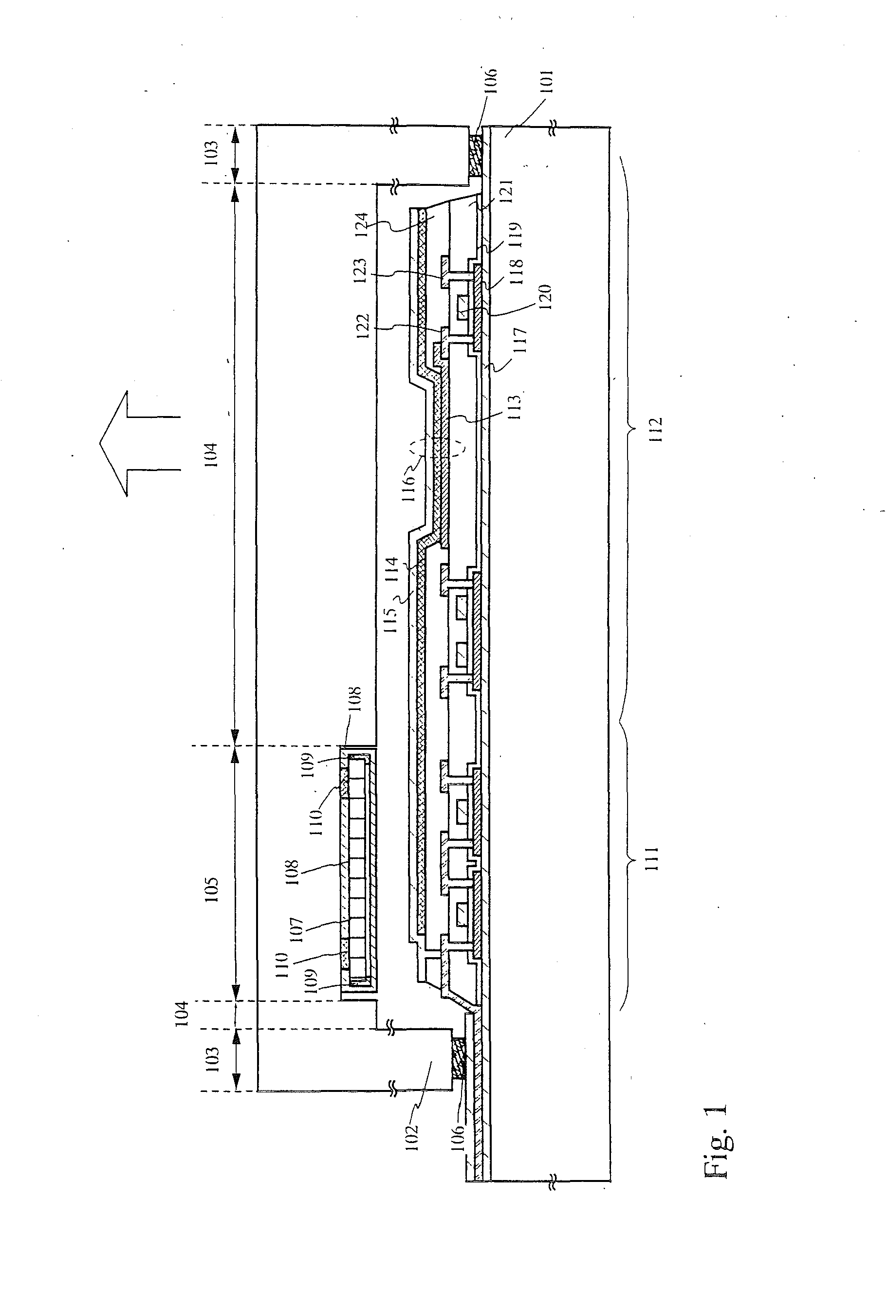
[0082]An embodiment mode of the present invention will be described using FIG. 1. FIG. 1 is a cross sectional view of an active matrix display device using an organic light emitting element.

[0083]A driver circuit portion 111 and a pixel portion 112 which are composed of TFTs are formed on a first substrate (element substrate) 101.

[0084]Substrates made of glass such as barium borosilicate glass, aluminoborosilicate glass, or quartz glass are used as the first substrate and the second substrate (sealing substrate) 102.

[0085]The surface of the second substrate is processed by an abrasive machining method and selectively shaved. By this processing, the surface of the second substrate has a first region 103, a second region 104, and a third region 105. The first region is a surface to which a layer having adhesion is adhered. When viewed from a rear surface of the second substrate, the first region is protruded in a convex shape relative to the second region and the third region.

[0086]An...

embodiment mode 2

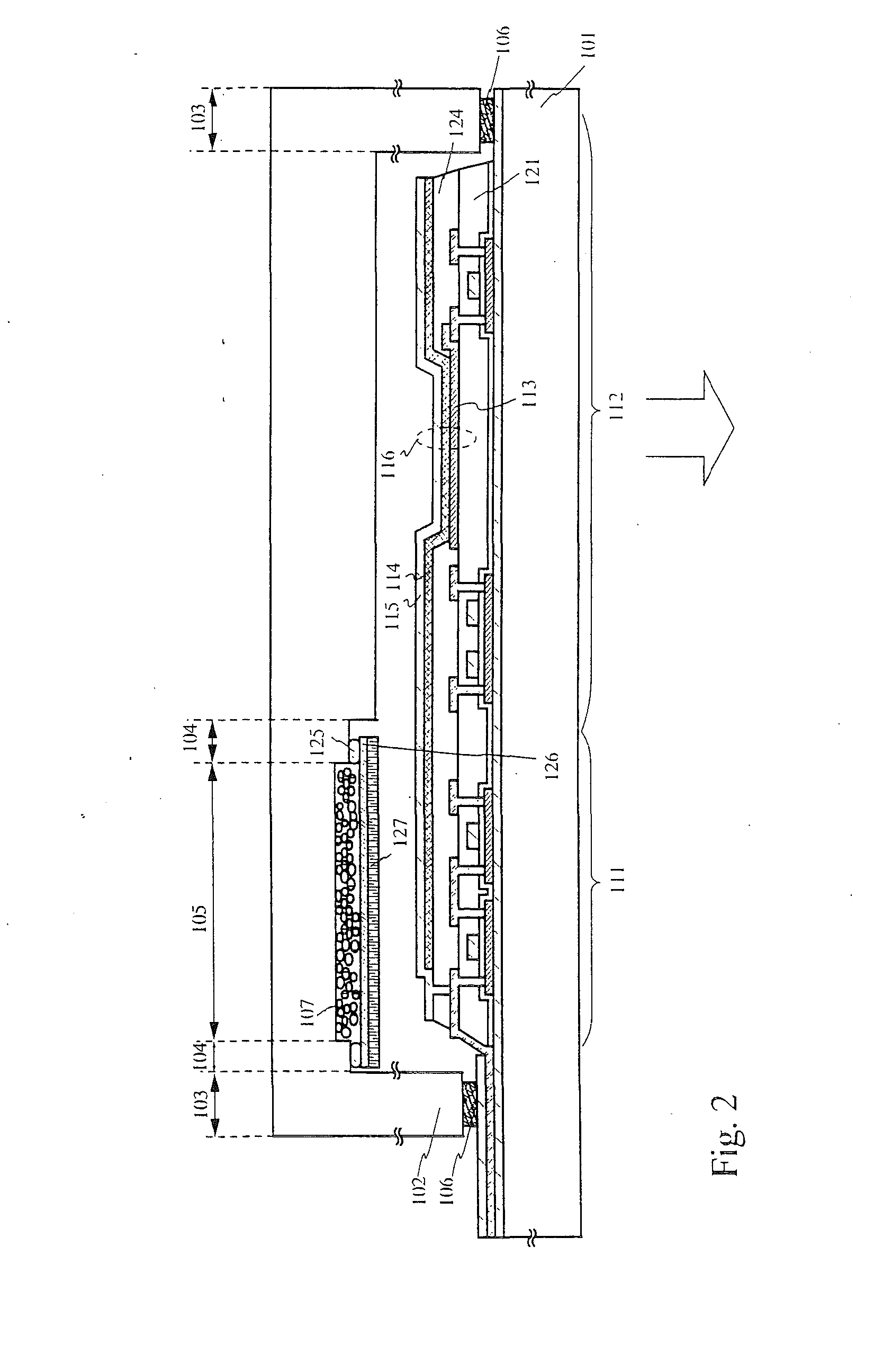
[0112]In this embodiment mode, an example where a dry agent and a permeable film are provided over a driver circuit portion is indicated. In this embodiment mode, points which are different from Embodiment Mode 1 will be described in detail. This embodiment mode will be described using a cross sectional view of FIG. 2. FIG. 2 is a cross sectional view of an active matrix display device using an active matrix organic light emitting element. Shown in the drawing is a driver-circuit-integrated structure in which a pixel portion 112 and a driver circuit portion 111 are formed on the same substrate.

[0113]Substrates made of glass can be used as a first substrate 101 and a second substrate 102.

[0114]In this embodiment mode, a granular material is used for a dry agent 107. When the dry agent is granular, a surface area thereof is increased and thus it is easier to absorb moisture. It is desirable that a particle size of the dry agent is set to be 10 μm to 80 μm. In this embodiment mode, the...

embodiment mode 3

[0122]This embodiment mode will be described using FIG. 3. As shown in FIG. 3, in a display device in which an organic light emitting element 116 is provided, minute unevennesses are formed on the surface of a substrate onto which light emitted from the organic light emitting element is outputted. Hereinafter, this embodiment mode will be described in detail.

[0123]In this embodiment mode, the organic light emitting element 116 has a structure in which a cathode 113, an organic compound layer 114, and an anode 115 are laminated in order, and light from the organic light emitting element 116 is emitted to the side indicated by an arrow in the drawing. In other words, a user views an image from a second substrate 102 side. At this time, outside light is reflected at the interface between the second substrate 102 and a sealed space and in an interface between the second substrate and air. Thus, unwanted reflection of an ambient background view is caused. In order to prevent such a pheno...


PUM


Abstract

In a display device using an organic light emitting diode (OLED), the occurrence of a dark spot and peeling of a cathode due to moisture are suppressed. An outer edge portion of a sealing substrate (second substrate) (102) is made to have a convex shape and a gap between the sealing substrate and an element substrate are controlled by means of this convex region. Thus, since it is not required that a layer (106) having adhesion for bonding together the sealing substrate and the element substrate has a function for controlling the gap, the thickness of the layer can be minimized. Therefore, the amount of moisture which is transmitted through the layer (having adhesion) made of an organic material and penetrated in a sealed region can be reduced.

Description

CROSS-REFERENCE TO RELATED APPLICATIONS[0001]This application is a continuation of U.S. application Ser. No. 10 / 821,927, filed Apr. 12, 2004, now pending, which is a divisional of U.S. application Ser. No. 10 / 062,294, filed Jan. 31, 2002, now U.S. Pat. No. 6,724,150, which claims the benefit of a foreign priority application filed in Japan as Serial No. 2001-026176 on Feb. 1, 2001, all of which are incorporated by reference.BACKGROUND OF THE INVENTION[0002]1. Field of the Invention[0003]The present invention relates to a display device using an organic light emitting element and a manufacturing method thereof, and more particularly to a display device using an organic light emitting element capable of keeping a stable light emitting property for a long period.[0004]Note that the organic light emitting element in this specification indicates an element in which an organic compound layer is sandwiched between two electrodes to produce light emission. As the organic light emitting elem...

Claims


Application Information

Patent Timeline
Patent Type & Authority Applications(United States)
IPC IPC(8): H01L51/52H01L27/32H01L51/00G09G3/32H01L51/56
CPCH01L51/5246H01L2251/558H01L27/3251H01L51/0096G09G3/3233G09G2300/0842G09G2310/0251Y02E10/549Y02P70/50H10K59/12H10K59/17H10K50/841H10K50/8426H10K50/846H10K50/85H10K50/86H10K71/00H10K2102/3026H10K59/127H10K77/10H10K2102/351
Inventor MARUYAMA, JUNYAYAMAZAKI, SHUNPEI
Owner SEMICON ENERGY LAB CO LTD
Why Eureka
Try Eureka