
Digital output clock generation

a digital output clock and clock signal technology, applied in the direction of pulse automatic control, pulse manipulation, electrical apparatus, etc., can solve the problems of complex interfaces, complexity and overhead associated with such complex interfaces, and it is difficult or even impossible to introduce such delay elements based on layout constraints of application boards, so as to achieve easy and efficient production, the effect of reducing the cost of design and tim

Inactive Publication Date: 2015-06-11
ARM LTD
View PDF11 Cites 0 Cited by
  • Summary
  • Abstract
  • Description
  • Claims
  • Application Information

AI Technical Summary

Benefits of technology

The present techniques describe a method for creating and testing a circuit layout using digital implementation techniques. This method involves using standard digital tools to select and place components in the circuit, and to generate clock signals for the circuit. This approach reduces design and implementation costs and avoids the need for late-stage adjustment of the circuit. The method also includes a method for generating a 90° phase shifted version of a clock signal, which can be useful in some cases. Overall, the method simplifies the process of creating and testing a circuit layout, and improves the efficiency of the process.

Problems solved by technology

However, given that such delay elements will then typically be introduced at a relatively late stage in the development process, it can be very difficult or even impossible to introduce such delay elements depending on the layout constraints of the application board.
Contemporary highly densely integrated circuit boards further exacerbate these difficulties.
However the complexity and area overhead associated with such complex interfaces are justifiable only for very high performance interfaces like DDR.

Method used


Image

  • Digital output clock generation
  • Digital output clock generation
  • Digital output clock generation

Examples


Embodiment Construction

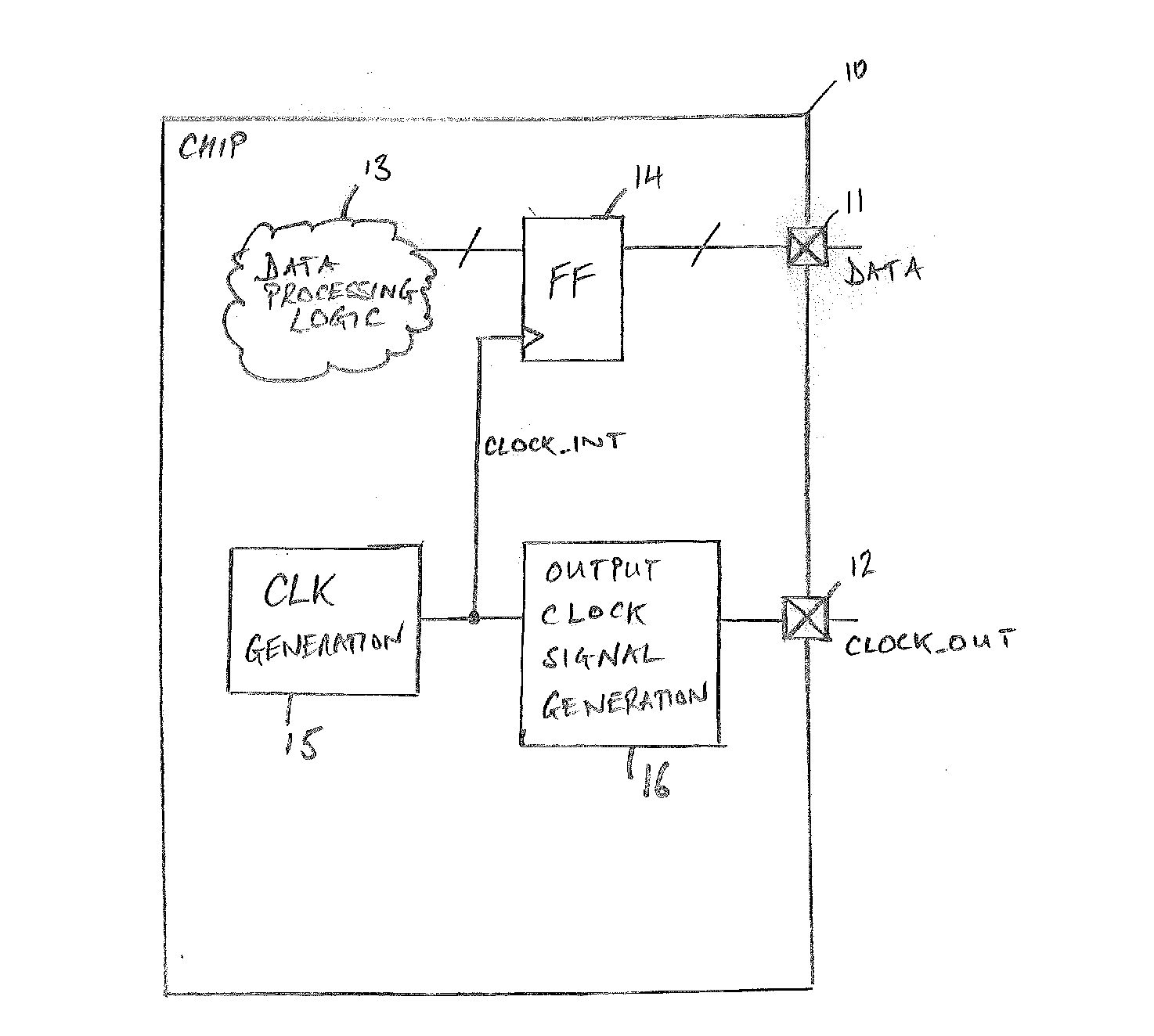
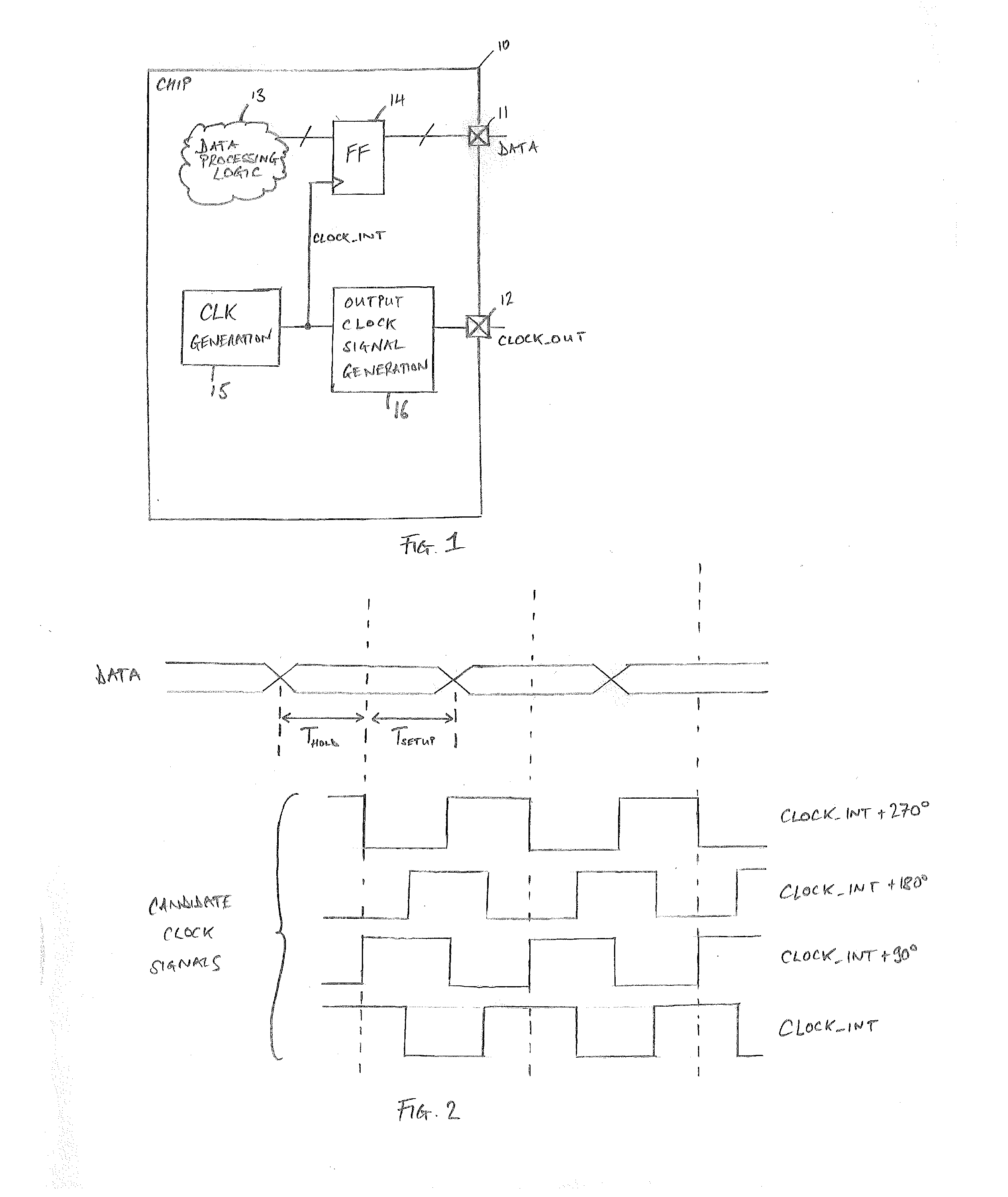
[0049]FIG. 1 schematically illustrates an integrated circuit embodied on a silicon chip 10. At the periphery of the chip there are provided a number of output pins, of which only two are illustrated here for clarity. A first pin 11 is provided as a data output path whilst a pin 12 is provided as a clock output path. The output clock signal provided at the pin 12 is in particular provided such that the data signal received via output pin 11 can be correctly interpreted, as will be discussed in more detail below with reference to FIG. 2. The integrated circuit generally comprises data processing logic 13 which generates data signals which are required to be exported off-chip. For this purpose the signals are passed via at least one flip-flop 14, coupled to the output pin 11. The timing of the output data signal thus depends on the timing of a clock signal CLOCK_INT which gates the operation of the flip-flop 14. The signal CLOCK_INT is generated by an on-chip clock generation unit 15. ...


PUM


Abstract

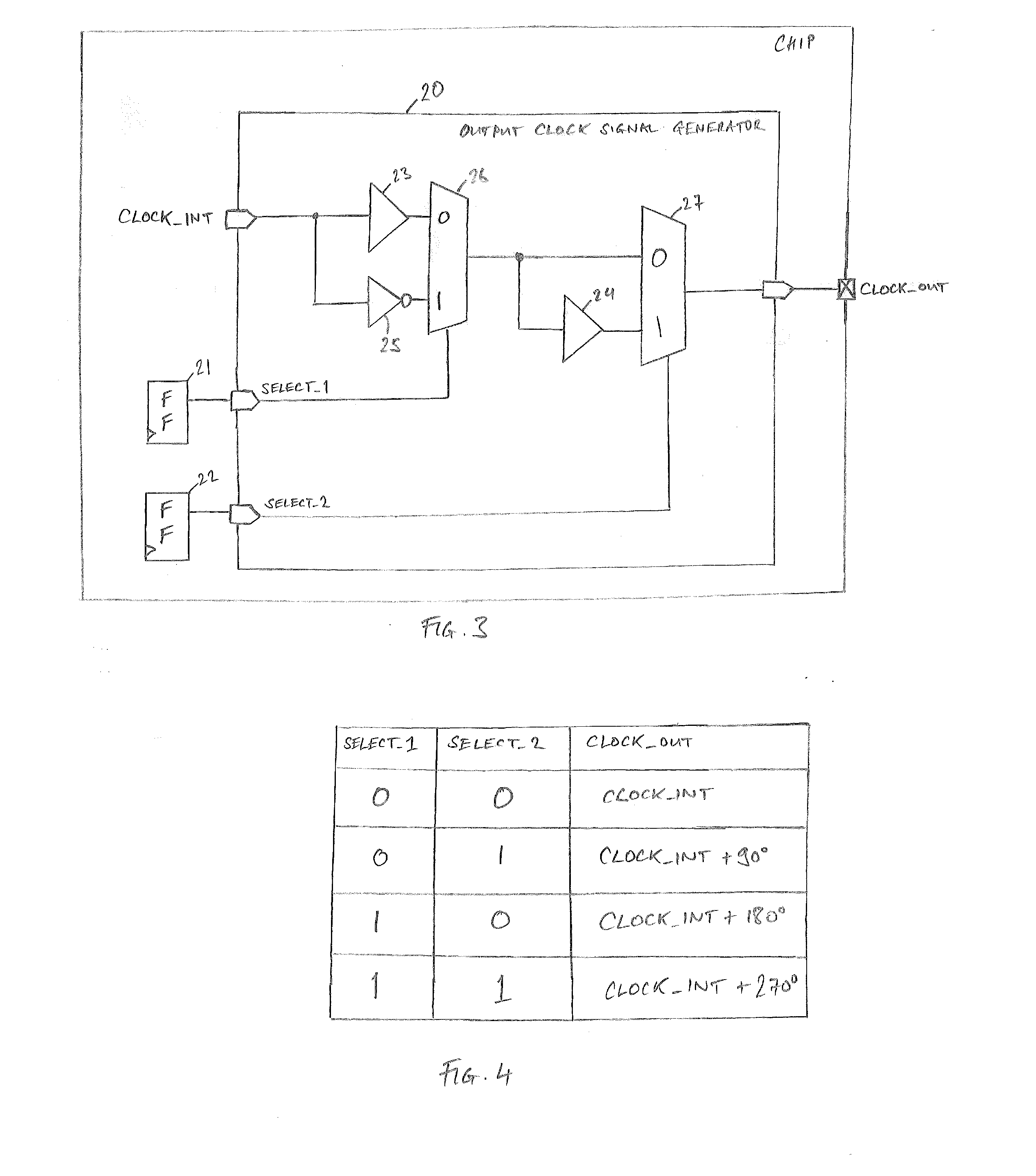
An on-chip clock signal generation apparatus is provided which is configured to generate an output clock signal to be passed off-chip in association with an output data signal. The apparatus comprises: an input configured to receive an input clock signal and clock phase generation circuitry configured to generate a plurality of candidate clock signals in dependence on the input clock signal. The candidate clock signals are phase-shifted with respect to one another. Selection circuitry is configured to select and output one of the candidate clock signals as the output clock signal in dependence on at least one selection signal. All components of the apparatus are embodied as digital components.

Description

BACKGROUND OF THE INVENTION[0001]1. Field of the Invention[0002]The present invention relates to integrated circuit technology. More particularly, this invention relates to on-chip clock signal generation.[0003]2. Description of the Prior Art[0004]It is known to provide a peripheral interface on an integrated circuit implemented as a silicon chip. This interface can be used to export data from the integrated circuit on-chip and such data signals will typically be accompanied by a clock signal also generated on-chip which has a specific relationship with the data signal, in particular indicating the points at which the data signal should be sampled. It is further known that the phase relationship between the data signal and its associated clock signal which are exported off-chip is critical if the data signal is to be correctly sampled.[0005]If it is discovered during the development of an on-chip integrated circuit that the output clock signal and the data signal are not well aligne...

Claims


Application Information

Patent Timeline
IPC IPC(8): H03L7/081H03L7/083
CPCH03L7/083H03L7/081H03K5/135
Inventor SWAMY, RAMNATH BOMMU SUBBIAH
Owner ARM LTD
Learn More