

Silicon carbide single crystal and method and apparatus for producing the same
a technology of silicon carbide and single crystal, which is applied in the direction of crystal growth process, polycrystalline material growth, chemically reactive gas growth, etc., to achieve the effect of high purity, low cost and easy acquisition
- Summary
- Abstract
- Description
- Claims
- Application Information
AI Technical Summary
Benefits of technology
Problems solved by technology
Method used
Image

Examples
example 1
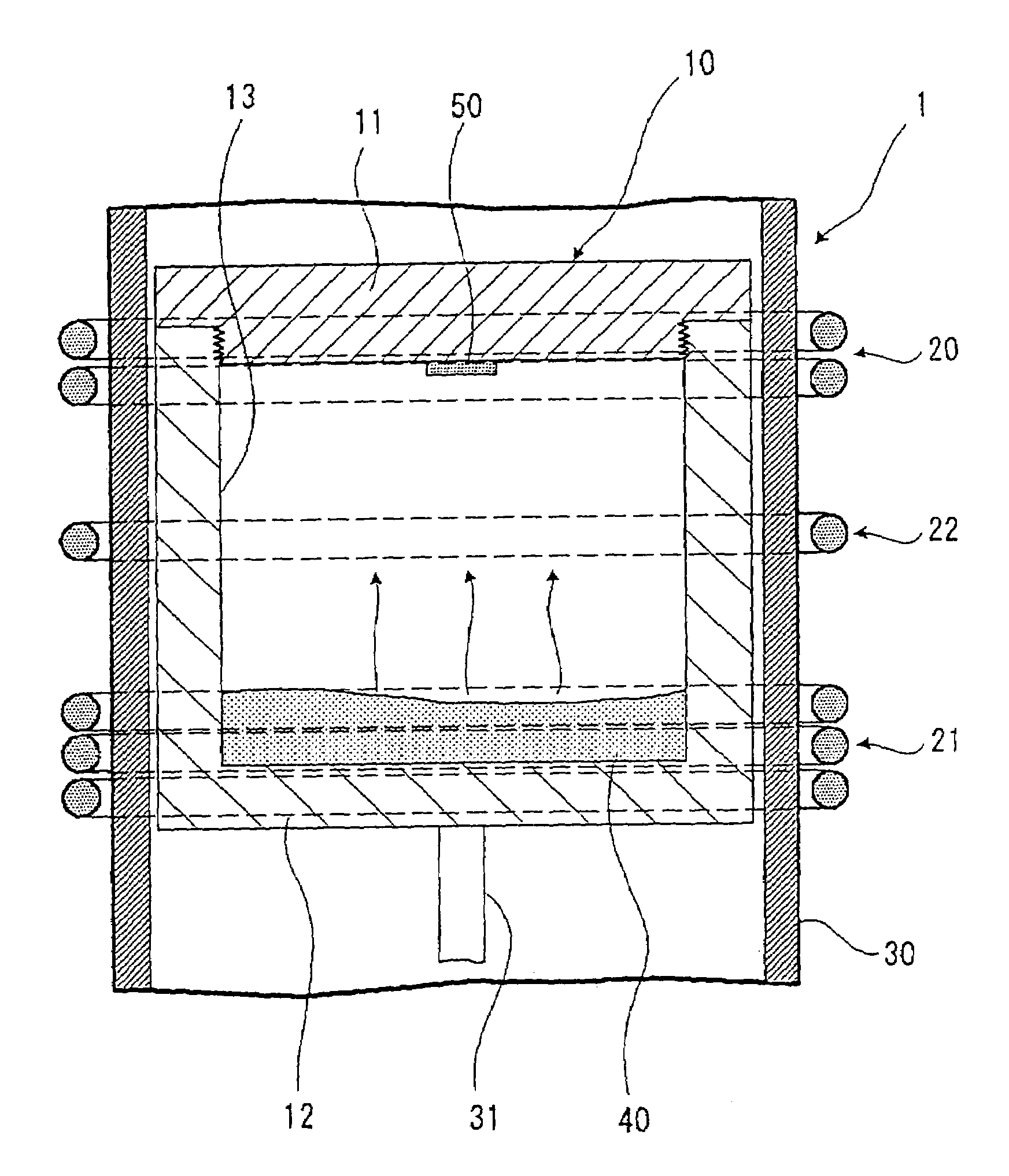
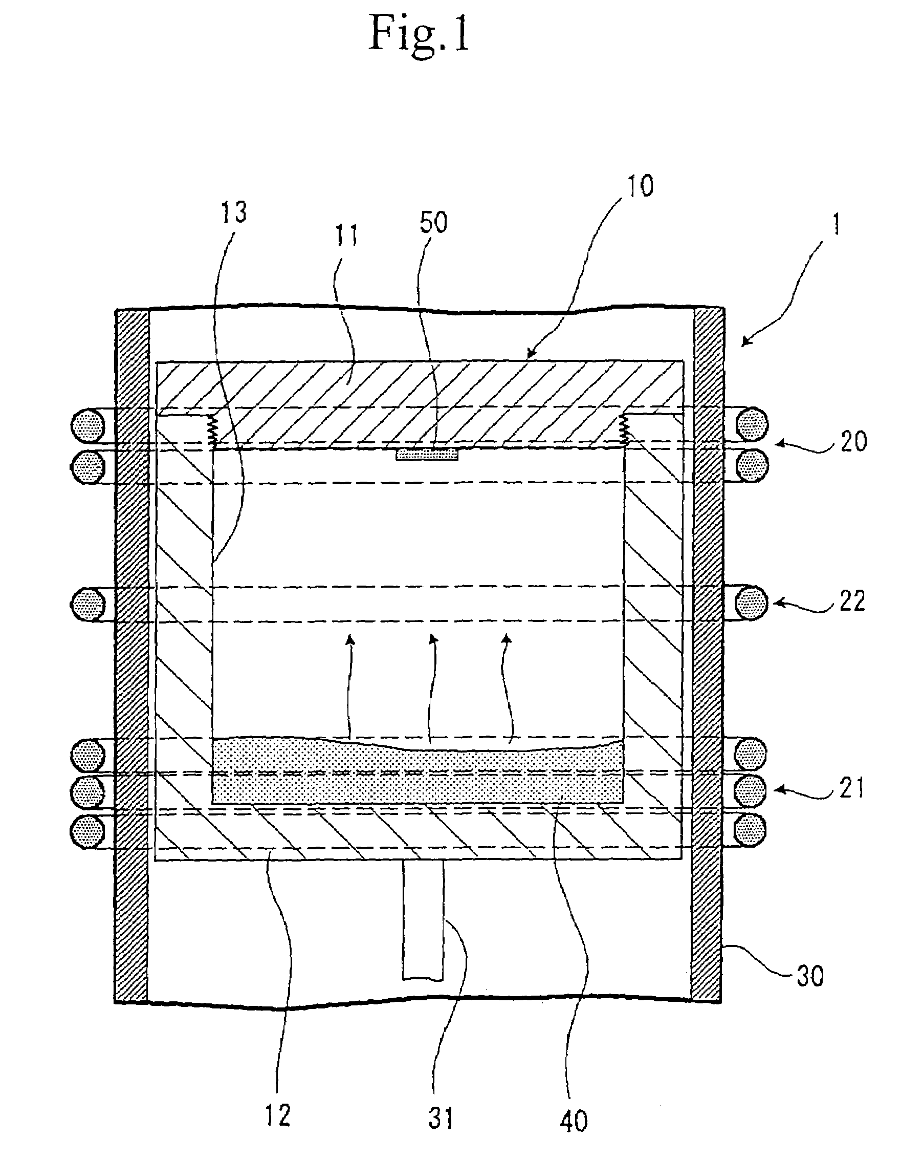
[0259]Using a silicon carbide single crystal production apparatus 1 shown in FIG. 1, a silicon carbide single crystal was produced. Use of the silicon carbide single crystal production apparatus 1 leads to execution of the silicon carbide single crystal production method of the present invention.
[0260]The silicon carbide single crystal production apparatus 1 comprises a graphite crucible 10 having a vessel body 12 capable of accommodating a sublimation raw material 40 and a cover body 11 which can be attached to and detached from the vessel body 12 by spiral fitting, and in which, when installed on the vessel body 12, a seed crystal 50 of a silicon carbide single crystal can be placed approximately at the center of a surface facing the sublimation raw material 40 accommodated in the vessel body 12; a supporting rod 31 fixing the graphite crucible 10 to inside of a quartz tube 30; a first induction heating coil 21 placed at a part which is on the outer periphery of the quartz tube an...
example 2
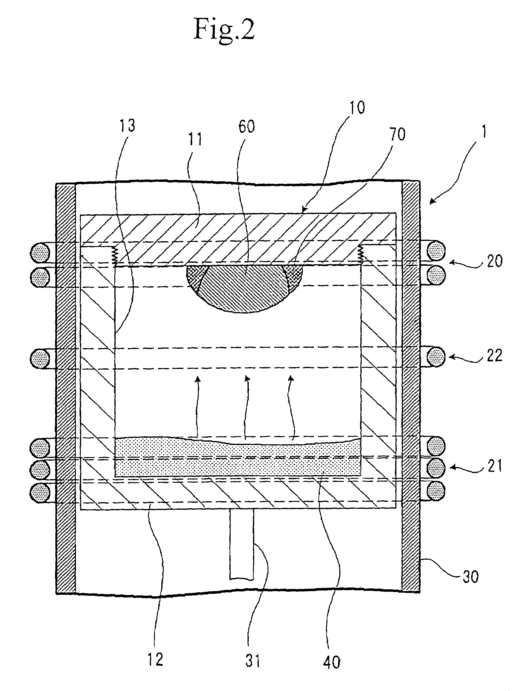
[0267]The same procedure as in Example 1 was conducted except that the graphite crucible 10 was changed to a graphite crucible 10 shown in FIG. 4 in Example 1. As a result, the same result as in Example 1 was obtained. The graphite crucible 10 shown in FIG. 4 differs from the graphite crucible 10 shown in FIG. 1 used in Example 1 only in that an inside region forming part 15 is provided in the cover body 11. The inside region forming part 15 is, as shown in FIG. 4, a cylinder having the above-mentioned inside region on which a seed crystal of a silicon carbide single crystal is placed as the bottom surface, and one end of which is exposed to outside of the graphite crucible 10. The material of inside region forming part 15 had a heat conductivity of 117 J / m / s / ° C. (W / m·K), and the material of the cover body 11 other than inside region forming part 15 had a heat conductivity of 129 J / m / s / ° C. (W / m·K).
[0268]In the case of Example 2, since the above-mentioned inside region is formed of...
example 4
[0271]The same procedure as in Example 1 was conducted except the following point in Example 1. Namely, the resulted silicon carbide powder had 6H and an average particle size of 300 μm, and the seed crystal 50 of a silicon carbide single crystal is a 15R wafer (diameter: 40 mm, thickness 0.5 mm) obtained by cutting the bulk silicon carbide single crystal obtained in Example 1 and mirror-polishing the whole surface.
[0272]Current of 20 kHz was flown through a first induction heating coil 21 to heat, and current of 40 kHz was flown through a second induction heating coil 20 to heat to increase the temperature. The lower part of the graphite crucible 10 (part accommodating the sublimation raw material 40) was heated to 2312° C., and the upper part of the graphite crucible 10 (place on which the seed crystal 50 of a silicon carbide single crystal is placed in the cover body 11) was heated to 2290° C., respectively. In this operation, the feeding powder to the first induction heating coi...
PUM
| Property | Measurement | Unit |
|---|---|---|
| temperature | aaaaa | aaaaa |
| atomic number | aaaaa | aaaaa |
| temperature | aaaaa | aaaaa |
Abstract
Description
Claims
Application Information