Nanostructured microelectrodes and biosensing devices incorporating the same

a biosensor and microelectrode technology, applied in the field of nanostructured microelectrodes and biosensors incorporating the same, can solve the problems of limited implementation of such devices, difficult to work with nanoscale electrodes, and low detection limits, and achieve easy integration into existing manufacturing facilities, promote the availability of target molecules, and facilitate work

Active Publication Date: 2015-06-18
THE GOVERNING COUNCIL OF THE UNIV OF TORONTO
View PDF2 Cites 5 Cited by
  • Summary
  • Abstract
  • Description
  • Claims
  • Application Information

AI Technical Summary

Benefits of technology

The invention features a new type of microelectrode structure, called NMEs (also known as nanowires), that can be used for biosensing applications. These NMEs have the ability to attach to probe molecules and promote easy accessibility of target molecules for hybridization or protein-to-protein binding. The NMEs can be manufactured using existing silicon CMOS foundry fabrication procedures, making them versatile, robust, and easy to work with. The technical effects of the invention include improved precision in microelectrode size and shape control, greater flexibility in nanotexturing, and the ability to select the NME material, allowing for customization of the NME system for different experimental parameters. The NMEs are also compatible with electrocatalytic electrochemistry and can be easily integrated into existing manufacturing facilities.

Problems solved by technology

However, spreading the reach of the genomics revolution to the patient bedside demands cost effective tools for individual biomarker profiling assessed relative to a posited disease state.
The challenges that have limited the implementation of such devices primarily stem from the difficulty of obtaining very low detection limits in the presence of high background noise levels present when complex biological samples are assayed, and the challenge of generating multiplexed systems that are highly sensitive and specific.
Working with nanoscale electrodes, however, is significantly more challenging, as fabrication is typically labour-intensive, insufficiently reproducible, and the currents obtained from such structures are typically difficult to measure accurately.
Manufacturing arrays of nanowire electrodes, however, is non-trivial.
However, this type of electrode cannot be incorporated into an array-based format for multiplexed experiments.
Existing methods that offer the specificity and sensitivity to profile clinical samples are typically costly, slow and serial.

Method used


Image

  • Nanostructured microelectrodes and biosensing devices incorporating the same
  • Nanostructured microelectrodes and biosensing devices incorporating the same
  • Nanostructured microelectrodes and biosensing devices incorporating the same

Examples


example 1

Parameters for Manufacturing NMEs

[0079]In this example, Pd was used as an electrode material. To investigate the time-dependence of the electrodeposition, the structures of the Pd NMEs being electrodeposited were monitored as a function of time. Time-dependent electrodeposition experiments were performed at −100 mV using 0.5 M HCl as supporting electrolyte. Pd structures were formed for (a) 25, (b) 50, (c) 125, (d) 250, and (e) 500 s. After 50 s, structures with average diameters of 1.3 μm and heights of 0.5 μm were observed, and after 500 s the Pd electrodes were typically 8 μm and 5 μm in diameter and height. The smaller structures made with shorter deposition times typically exhibited depressions in the center of the microelectrodes, which may indicate that nucleation occurs preferentially at the boundary of the aperture.

[0080]Another controllable parameter that may influence the final structure of the NME is the deposition potential. Specifically, the size and surface morphology...

example 2

Direct Profiling of Prostate Cancer Biomarkers in Tumor Tissue Using a Multiplexed Nanostructured Microelectrode Integrated Circuit

[0086]Materials and Methods

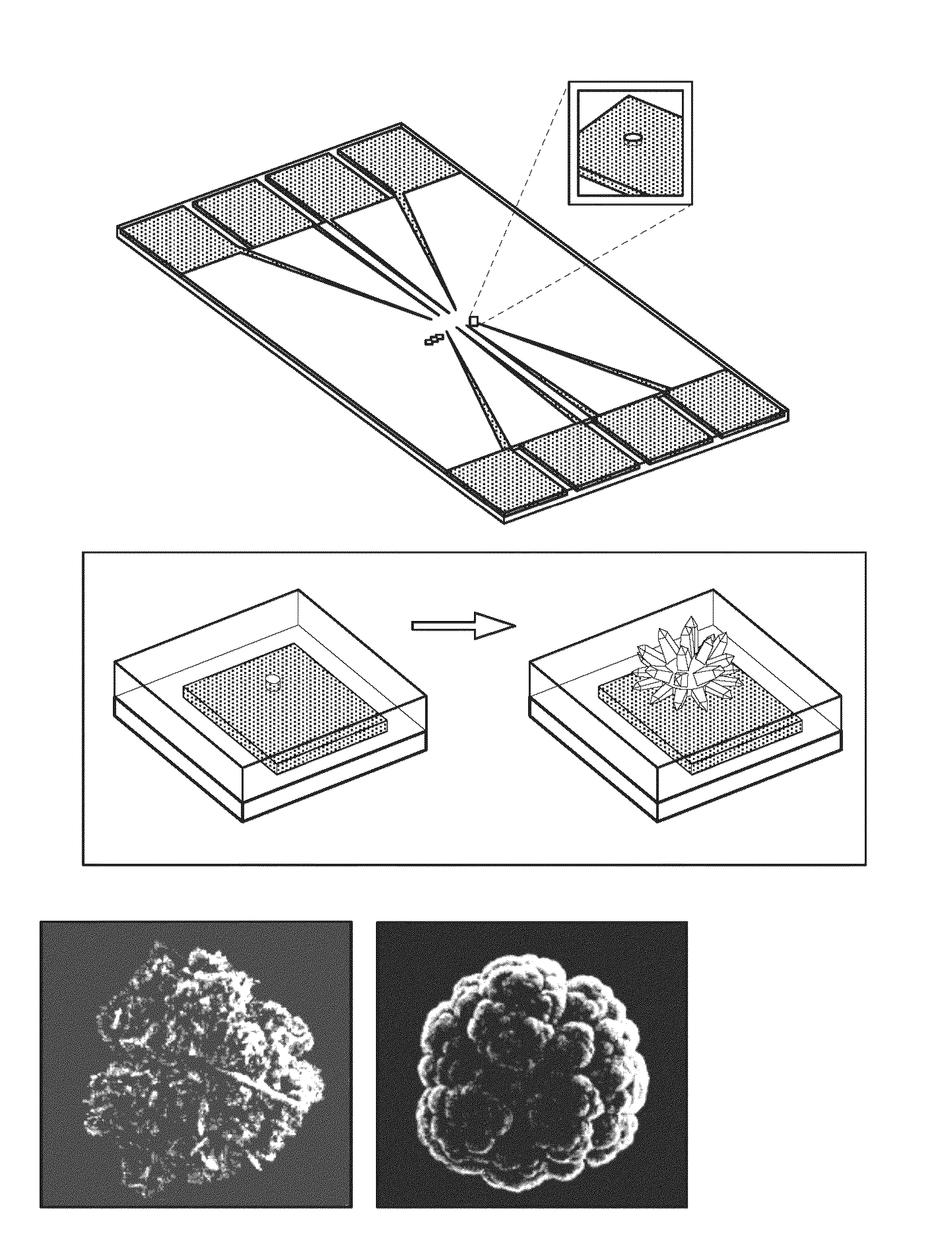
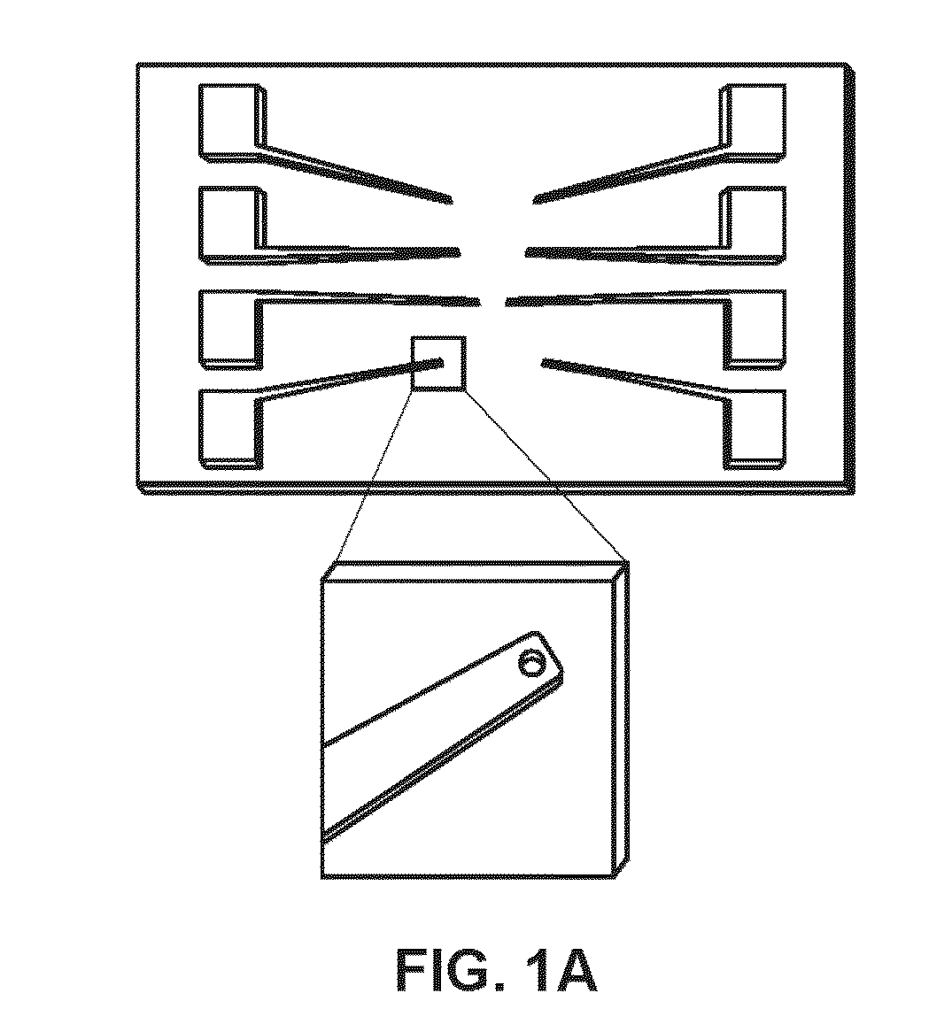
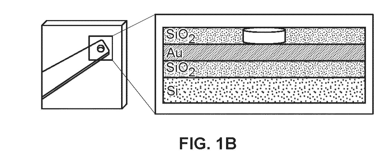
[0087]Chip Fabrication.

[0088]The chips were fabricated at the Canadian Photonics Fabrication Center. 3″ silicon wafers were passivated using a thick layer of thermally grown silicon dioxide. A 350 nm gold layer was deposited on the chip using electron-beam assisted gold evaporation. The gold film was patterned using standard photolithography and a lift-off process. A 500 nm layer of insulating silicon dioxide was deposited using chemical vapor deposition. 500 nm apertures were imprinted on the electrodes using standard photolithography, and 2 mm×2 mm bond pads were exposed using standard photolithography.

[0089]Fabrication of Nanostructured Microelectrodes.

[0090]Chips were cleaned by rinsing in acetone, IP A, and DI water for 30 s and dried with a flow of nitrogen. All electrodeposition was performed at room temperature with a B...

example 3

Direct, Electronic MicroRNA Detection Reveals Differential Expression Profiles in 30 Minutes

[0116]Materials and Methods

[0117]Materials.

[0118]6-mercapto-1-hexanol (97% MCH), hexaamine ruthenium chloride (99.9+%), potassium ferricyanide (99%), and palladium (II) chloride(99.9+%) were purchased from Sigma-Aldrich Canada Ltd (Oakville, ON), perchloric acid (70%), acetone (ACS grade) and isopropyl alcohol (IPA, ACS grade) were obtained from EMD (Gibbstown, N.J.). Thiolated PNA oligomers were obtained from Biosynthesis Inc (Lewisville, Tex.) with HPLC purified grade. PNA probes a Cys-Gly dipeptide at their N-terminus. Gly acts as a spacer, while Cys provides free thiol for immobilization on the electrode surface. Synthetic microRNAs (5′ end phosphorylated and HPLC purified) were obtained from Euro fins MWG Operon (Huntsville, Ala.). All PNA and RNA sequences are shown in table 51 provided in the supporting information.

[0119]Chip Fabrication.

[0120]The chips were fabricated at the Canadian ...


PUM


Abstract

Nanostructured microelectrodes and biosensing devices incorporating the same are disclosed herein.

Description

CROSS-REFERENCE TO RELATED APPLICATIONS[0001]This application is a divisional of U.S. patent application Ser. No. 13 / 061,465 which is a United States National Stage Application filing under 35 U.S.C. §371 of International Application No. PCT / CA2009 / 001212, filed on Sep. 1, 2009, which claims the benefit of priority of U.S. Provisional Patent Application Ser. No. 61 / 093,667, filed on Sep. 2, 2008, entitled Nanostructured Microelectrodes and Biosensing Devices Incorporating the Same, now expired, the contents of each of which is hereby incorporated by reference herein in its entirety. International Application No. PCT / CA2009 / 001212 was published under PCT Article 21(2) in English.SEQUENCE LISTING[0002]The instant application contains a Sequence Listing which has been submitted electronically as a text file in ASCII format and is hereby incorporated by reference in its entirety. Said text file, created on Feb. 20, 2015, is named 109904-0004-302.txt and is 6,000 bytes in size.BACKGROUND...

Claims


Application Information

Patent Timeline
Patent Type & Authority Applications(United States)
IPC IPC(8): G01N27/327
CPCG01N27/3275G01N27/3272G01N27/3278G01N33/5438Y10S977/754Y10S977/925G01N27/30
Inventor SOLEYMANI, LEYLAFANG, ZHICHAOKELLEY, SHANASARGENT, EDWARDTAFT, BRADFORD
Owner THE GOVERNING COUNCIL OF THE UNIV OF TORONTO
Why Eureka
Try Eureka