Liquid crystal panel and manufacturing method thereof

a technology of liquid crystal panels and manufacturing methods, which is applied in the manufacture of electrode systems, electric discharge tubes/lamps, instruments, etc., can solve the problems of uneven edges of alignment films, difficult control of the size of alignment films, and difficulty in controlling the diffusion of alignment liquids. , to achieve the effect of reducing the distance between the edge and preventing the diffusion of alignment liquids

Inactive Publication Date: 2015-06-18
SHENZHEN CHINA STAR OPTOELECTRONICS TECH CO LTD
View PDF4 Cites 12 Cited by
  • Summary
  • Abstract
  • Description
  • Claims
  • Application Information

AI Technical Summary

Benefits of technology

[0006]An object of the present invention is to provide a structure to prevent an alignment liquid from being spread to the sealant so as to affect the adhesion of the sealant.
[0007]For achieving the above-mentioned technical solution, the present invention proposes a LC panel and the LC panel comprises a top substrate, a bottom substrate and at least one sealant. The bottom substrate comprises a display region, a non-display region, a first limiting component and a second limiting component. The non-display region is adjacent to the display region. The first limiting component is formed to be a convex at an edge of the non-display region. The second limiting component is formed to be a concave between the first limiting component and the non-display region. When an alignment film is coated on the bottom substrate, the alignment film will not be spread to the non-display region through assembling the first limiting component and the second limiting component.
[0008]Another object of the present invention is to provide a liquid crystal (LC) panel manufacturing method to produce a structure to prevent the diffusion of the alignment liquid and decrease the distance between the edge of the display region and the edge of the panel so as to achieve the design of an ultra-thin frame.
[0009]For achieving the above-mentioned technical solution, the present invention proposes an LC panel manufacturing method, wherein the manufacturing method comprises following steps: a step of respectively stacking a plurality of thin films on a top substrate and a bottom substrate; a step of retaining a portion of the thin films on a side of a sealant to form a first limiting component when forming a plurality of the thin films on the bottom substrate; a step of etching a plurality of the thin films on the bottom substrate to form a second limiting component; and a step of coating an alignment film on the bottom substrate to form an alignment layer. By a conjunction of the first limiting component and the second limiting component, during the process to coat the alignment film, the first limiting component and the second limiting component are utilized to prevent the alignment film from being spread to an area of the sealant so as to avoid the alignment film overlapping the sealant.
[0010]According to the description above, the advantages of the present invention is: by the structure of the first limiting component and the second limiting component, the first limiting component and the second limiting component are utilized to prevent the alignment film from being spread to the area of the sealant during the process for coating the alignment film. In other words, by the installation of the first limiting component and the second limiting component, the purpose of evenly coating the alignment film can be achieved and the distance between the edge of the display region and the edge of the panel can be decreased to easily accomplish the purpose of the ultra-thin frame.

Problems solved by technology

However, considering the properties that the insulativity of the PI and the adhesive force of the sealant are inadequate, when the alignment liquid is coated to form the alignment layer, it is not easy to control the diffusion of the alignment film, leading to a disadvantages that the edge of the alignment film is uneven and the size thereof is not easy to control.
When the alignment film is spread to the area of the sealant, the strength of the sealant will be decreased and the quality of the sealant is affected.
In addition, because the thickness of the alignment film is uneven, the problem of the uneven alignment would occur to affect the display quality.
Moreover, because the step formed by the groove or the bump is too small, the alignment liquid is easy to be spread over the groove or the bump and the design of the groove or the bump is failed.

Method used


Image

  • Liquid crystal panel and manufacturing method thereof
  • Liquid crystal panel and manufacturing method thereof
  • Liquid crystal panel and manufacturing method thereof

Examples


Embodiment Construction

[0017]In the following detailed description of the preferred embodiments, reference is made to the accompanying drawings which form a part hereof, and as shown by way of illustration specific embodiments in which the invention may be practiced. As such, the directional terminology is used for purposes of illustration and is in no way limiting the present invention.

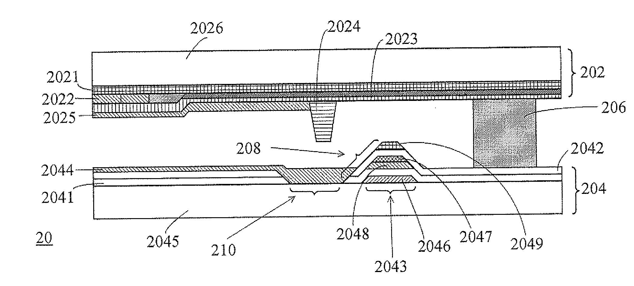
[0018]FIG. 2 is a cross-sectional structure view illustrating a liquid display panel in a preferred embodiment of the present invention. As shown in FIG. 2, the LC panel 20 includes a top substrate 202, a bottom substrate 204 and a sealant 206. The top substrate 202 is a Color Filter (CF) and includes a Black Matrix (BM) 2021, a color filter layer 2022, a transparent conductive (also called Indium Tin Oxide, ITO) layer 2023, a Photo Spacer (PS)2024, a first alignment film 2025, a glass substrate 2026 and so on. The function of the BM 2021 in the top substrate 202 is to shelter light source and avoid the leakage of an emitt...


PUM

PropertyMeasurementUnit
areaaaaaaaaaaa
coloraaaaaaaaaa
angleaaaaaaaaaa

Abstract

A liquid crystal panel is provided herein and comprises a top substrate, a bottom substrate and at least one sealant. The bottom substrate comprises a display region, a non-display region, a first limiting component and a second limiting component. The non-display region is adjacent to the display region. The first limiting component is formed as a convex at an edge of the non-display region. The second limiting component is formed as a concave between the first limiting component and the non-display region. When an alignment film is coated on the bottom substrate, the alignment film will not be spread to the non-display region by a conjunction of the first limiting component and the second limiting component.

Description

FIELD OF THE INVENTION[0001]The present invention relates to a field of liquid crystal panels, and more particularly to a liquid crystal panel and a manufacturing method thereof.BACKGROUND OF THE INVENTION[0002]A liquid crystal (LC) panel is a significant component in the LC display. The LC panel includes an array substrate, a color film substrate and LCs, which are disposed between the array substrate and the color film substrate. The LCs are aligned by an alignment film coated on the array substrate and the color film substrate to control the arrangement of the LCs and provide a pre-tilt angle for the need of the LC display, so as to achieve the display result of the LC panel. The commonly used alignment film is made of polyimide (PI) material, and the PI material has properties such as high heat resistance, chemical solvents resistance, as well as good radiation and electricity insulativity, and so on.[0003]However, considering the properties that the insulativity of the PI and t...

Claims


Application Information

Patent Timeline
Patent Type & Authority Applications(United States)
IPC IPC(8): G02F1/1337G02F1/1368G02F1/1339
CPCG02F1/1337G02F2001/133776G02F1/1368G02F1/1339G02F1/133388G02F1/133776
Inventor SHIH, MINGHUNGLIAO, ZUOMIN
Owner SHENZHEN CHINA STAR OPTOELECTRONICS TECH CO LTD
Why Eureka
Try Eureka