Micro device transfer device and transfer method

A micro-device transfer, micro-device technology, applied in semiconductor devices, electric solid-state devices, semiconductor/solid-state device manufacturing, etc., can solve problems such as easily damaged chips, pollution, failure, etc., to prevent unnecessary interference and reduce use costs , the effect of improving the range of adaptation

Active Publication Date: 2020-12-25
WUHAN UNIV
View PDF12 Cites 2 Cited by
  • Summary
  • Abstract
  • Description
  • Claims
  • Application Information

AI Technical Summary

Problems solved by technology

However, the electric field and electrostatic interaction may affect the internal structure of the chip, thus limiting the practicality of the transfer device
Similarly, the patent with the publication number CN110753487A provides a device that utilizes the capillary action of the liquid water film to absorb the chip. Although this force is soft and not easy to damage the chip, water vapor is also likely to affect the internal structure of the chip.
The patents with publication numbers CN 110752167A and CN110797295A use the phase change or volume shrinkage and expansion of the photosensitive adhesive layer to control the adhesion and detachment of the chip respectively. However, in the process, the photosensitive adhesive layer will be greatly deformed under pressure. Improper operation of the pressure application process can easily damage the chip. In addition, the photosensitive adhesive is also likely to remain on the surface of the target chip, causing pollution
[0004] In addition, for some electronic devices such as chips with curvature on the surface, it is often difficult for existing chip transfer devices to form a good contact with the surface, which leads to instability or even failure in the process of adhesion and transfer.

Method used


Image

  • Micro device transfer device and transfer method
  • Micro device transfer device and transfer method
  • Micro device transfer device and transfer method

Examples


Embodiment 1

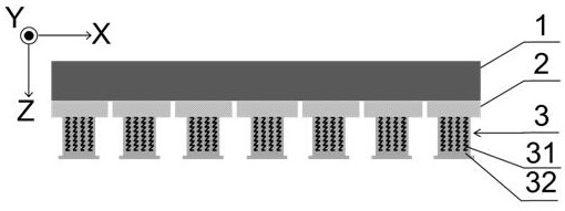
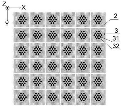
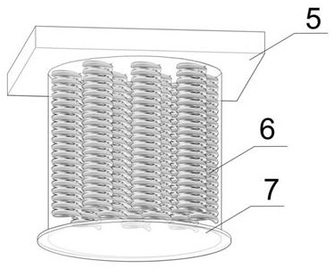
[0047] Such as Figure 1 to Figure 4 As shown, a micro-device transfer device is generally in the shape of a cube, including: a temperature-controlling substrate, a heat-insulating and insulating shape-adapting layer, and adhesive units arranged in multiple rows and columns. The adhesion unit includes an elastic body and a temperature control element group set in the elastic body for controlling its temperature. The elastic body of the adhesion unit is a micron-sized silicone rubber cylinder with a height of 10 microns and a diameter of 20 microns. The thickness of the column top sheet is 1 micron, The diameter is 24 microns; the internal temperature control element of the adhesion unit is a micron spiral column of metal material, and the spiral column is arranged in a hexagonal array to form a temperature control element group. A single spiral temperature control element is 8 microns in height and 4 in diameter. Microns.

[0048] Specifically, the morphology adaptation layer...

Embodiment 2

[0052] Based on the structural design of the controllable micro-device transfer device in Example 1, the shape adaptation layer can be replaced by a polyetheretherketone topological structure adaptation layer manufactured by additives, and the arrangement of the adhesion units can be replaced by a square arrangement, as shown in Figure 5 As shown, the internal temperature control element group of the adhesion unit is replaced by an array of micron wave-shaped temperature control elements made of ceramic material, and the elastomer can be replaced by ethylene-propylene rubber.

[0053] Specifically, the size of the adhesion unit is 10 microns in height and 15 microns in diameter, the thickness of the top sheet is 1 micron and 25 microns in diameter, and the size of a single internal temperature control element is 7 microns in height and 4 microns in width.

[0054] In the adhesion test of the adhesion unit, the test temperature ranges from 20 to 150 degrees Celsius.

Embodiment 3

[0056] Based on the structural design of the controllable micro-device transfer device in Example 1, the shape adaptation layer can be replaced by a polyether ether ketone topological structure adaptation layer manufactured by additives, and the arrangement of the adhesion units can be replaced by a square arrangement. The temperature control element group is an array of micron wave-shaped temperature control elements made of ceramic material, and the elastic body is ethylene-propylene rubber.

[0057] Specifically, the size of the adhesion unit is 11 microns in height and 14 microns in diameter, the thickness of the column top sheet is 1 micron and 24 microns in diameter, and the size of a single internal temperature control element is 8 microns in height and 5 microns in width.

[0058] In the adhesion test of the adhesion unit, the test temperature ranges from 20 to 160 degrees Celsius.


PUM


Abstract

The invention discloses a micro device transfer device and transfer method; the micro device transfer device comprises a temperature control substrate, a morphology adaptation layer and adhesion unitsarranged in an array; each adhesion unit comprises an elastomer and a temperature control element group arranged in the elastomer and used for controlling the temperature of the elastomer, and the elastomer of each adhesion unit is of a micron-scale columnar structure. The elastomer is made of an entropy elastic material, and the temperature control element group is electrically connected with the temperature control substrate. In the transferring process, according to the weight and the shape of a target transferring device, the target temperature of the corresponding adhesion unit is set through the temperature control substrate, and the device is picked up and transferred to the target position after being in good contact with the target device; the temperature control element group ispowered off, the adhesion units are separated from the target device, and device transfer is completed. The adhesive force can be adjusted as required, stress on the device in the transfer process can be basically prevented, and the device and method are particularly suitable for transfer of high-precision devices and ultrathin devices.

Description

technical field [0001] The invention belongs to the field of photoelectric technology and relates to a chip transfer technology, in particular to a micro device transfer device and a transfer method. Background technique [0002] With the development of electronic manufacturing technology, the miniaturization and cost reduction of electronic equipment also make the electronic devices in them develop in the direction of lighter, thinner and more efficient. Taking electronic chips as an example, since the first generation of chips in the 1950s, chip manufacturing technology has developed rapidly. For example, microchips with a size on the order of microns have great application prospects in display devices, mobile phones, and even living organisms. However, after the preparation is completed, how to quickly and stably transfer a large number of chips from the donor substrate to the receiving substrate for further operations without causing damage to the chip has become a probl...

Claims


Application Information

Patent Timeline
Patent Type & Authority Applications(China)
IPC IPC(8): H01L21/683H01L33/00
CPCH01L21/6835H01L33/00H01L2221/68363
Inventor 薛龙建汪鑫刘胜史哲坤
Owner WUHAN UNIV
Why Eureka
Try Eureka