

Electronic element sealing method and bonded substrate
Patent Information
- Authority / Receiving Office
- US · United States
- Current Assignee / Owner
- LAN TECHN SERVICE
- Publication Date
- 2015-06-18
Smart Images
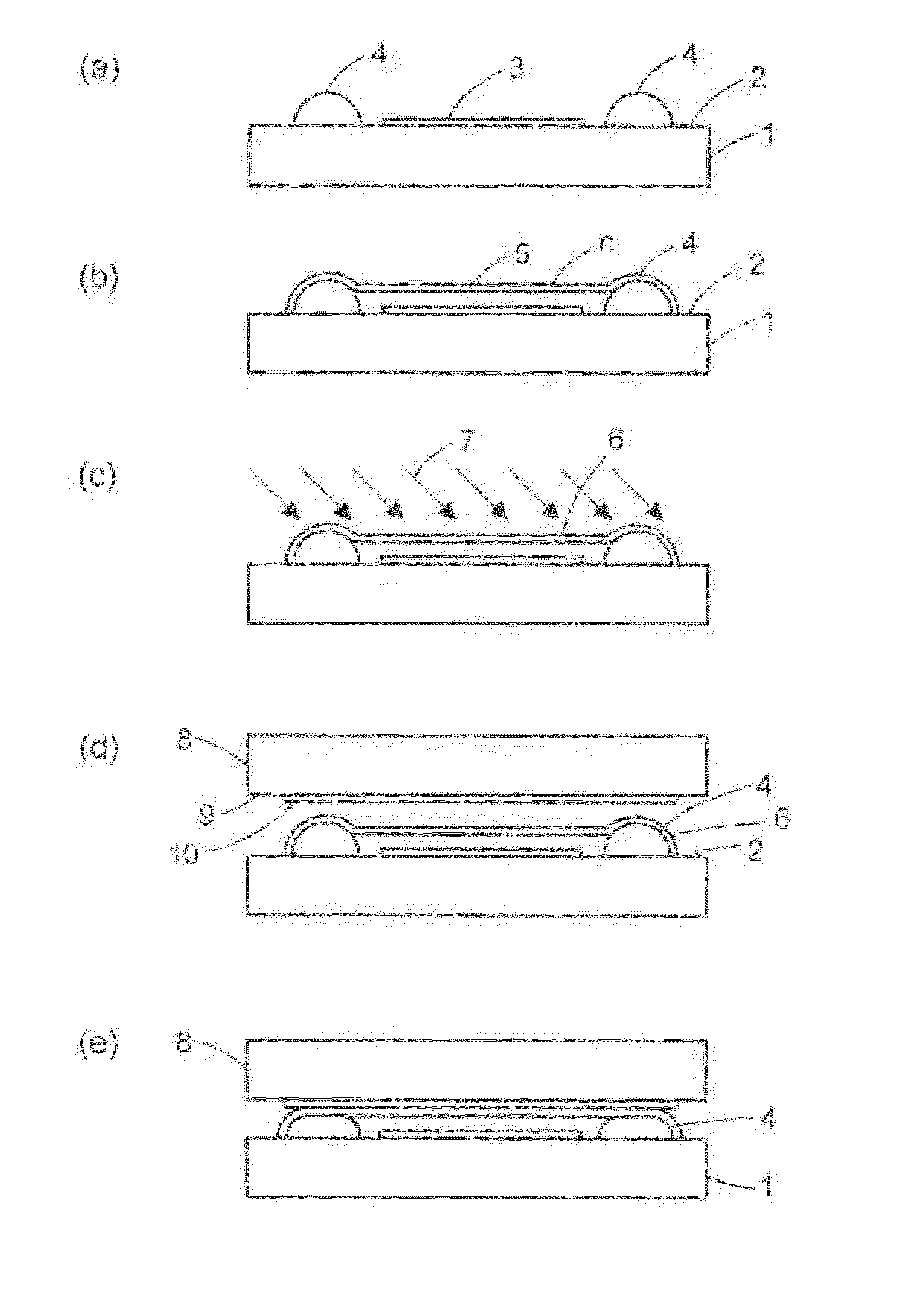
Figure 1 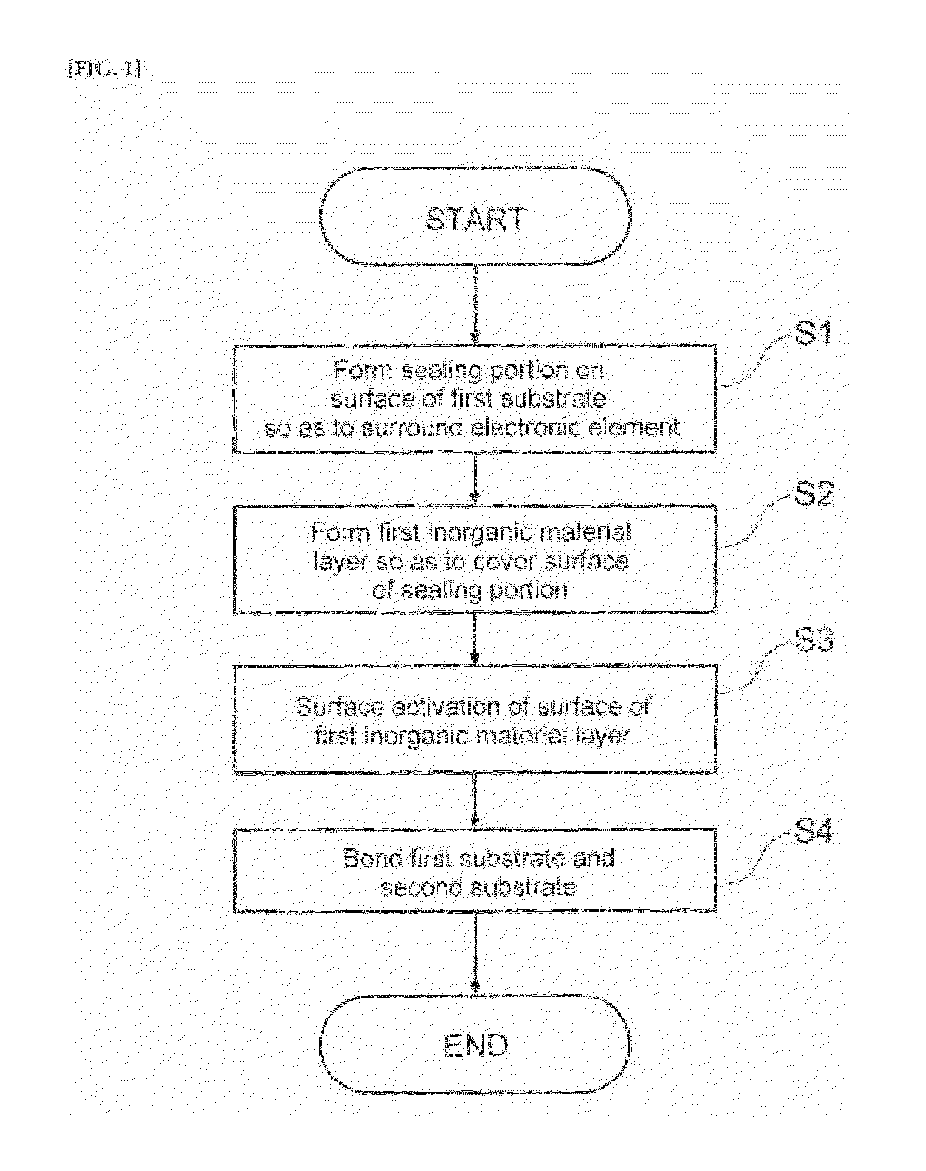
Figure 2 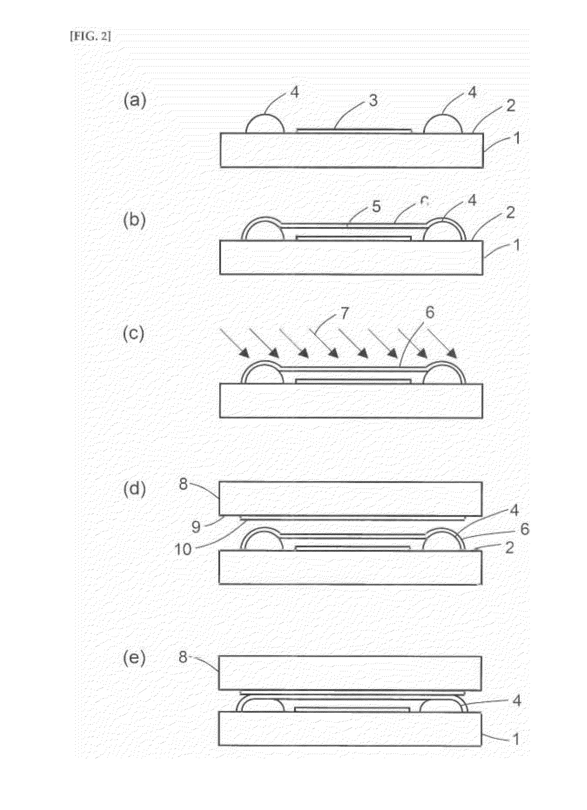
Figure 3
Abstract
Description
TECHNICAL FIELD
[0001] The present invention relates to a sealing method for an electronic element such as an organic electroluminescence element, and a bonded substrate for an electronic element.
[0002] Organic electroluminescence elements (organic EL elements) that make use of organic electroluminescence (organic EL) are composed of planar light-emitting layers consisting of organic compounds on a transparent substrate, and they have been developed for application to thin displays and the like. Compared to liquid crystal displays, organic EL displays making use of organic EL elements have a wider viewing angle, consume less power, and are soft and flexible enough to be bent, so they have high industrial value.
[0003] However, organic EL elements have the drawback that their function can deteriorate due to the active metals used as the electrodes reacting with water or oxygen and forming insulators. Therefore, the end surfaces of the substrates are often sealed with fritted glass as a m...