Microelectromechanical system and methods of use

a micro-electromechanical and mechanical technology, applied in the field of micro-electromechanical systems, can solve the problem that the dimensions of the fabricated structure often do not match the dimensions

Inactive Publication Date: 2015-06-25
PURDUE RES FOUND INC
View PDF4 Cites 36 Cited by
  • Summary
  • Abstract
  • Description
  • Claims
  • Application Information

AI Technical Summary

Benefits of technology

[0081]d) one or more displacement stopper(s) arranged to form a first displacement-stopping surface and a second displacement-stopping surface, wherein the first and second displacement-stopping surfaces limit travel of the movable mass in respective, opposite directions along the displacement axis to respective first and second distances away from the reference position, wherein the first distance is different from the second distance.

Problems solved by technology

However, when a MEMS device is fabricated, the dimensions of the structures fabricated often do not match the dimensions specified in the layout.

Method used


Image

  • Microelectromechanical system and methods of use
  • Microelectromechanical system and methods of use
  • Microelectromechanical system and methods of use

Examples


Embodiment Construction

[0164]Reference is also made to the following, the disclosure of each of which is incorporated herein by reference:[0165][A10] F. Li, J. V. Clark, “Self-Calibration for MEMS with Comb Drives: Measurement of Gap,” Journal of Microelectromechanical Systems, accepted May, 2012.[0166][B13] Clark, J. V., 2012, “Post-Packaged Measurement of MEMS Displacement, Force, Stiffness, Mass, and Damping”, International Microelectronics and Packaging Society.[0167][B14] Li. F, Clark, J. V., 2012, “Self-Calibration of MEMS with Comb Drives: Measurement of Gap”, Journal of Microelectromechanical Systems, December 2012.[0168][D12] J. V. Clark, “Post-Packaged Measurement of MEMS Displacement, Force, Stiffness, Mass, and Damping”, International Microelectronics and Packaging Society, March (2012).

[0169]Symbols for various quantities (e.g., Agap) are used herein. Throughout this disclosure, italic and non-italic variants of each of these symbols (e.g., “Δgap” and “Δgap”) are equivalent.

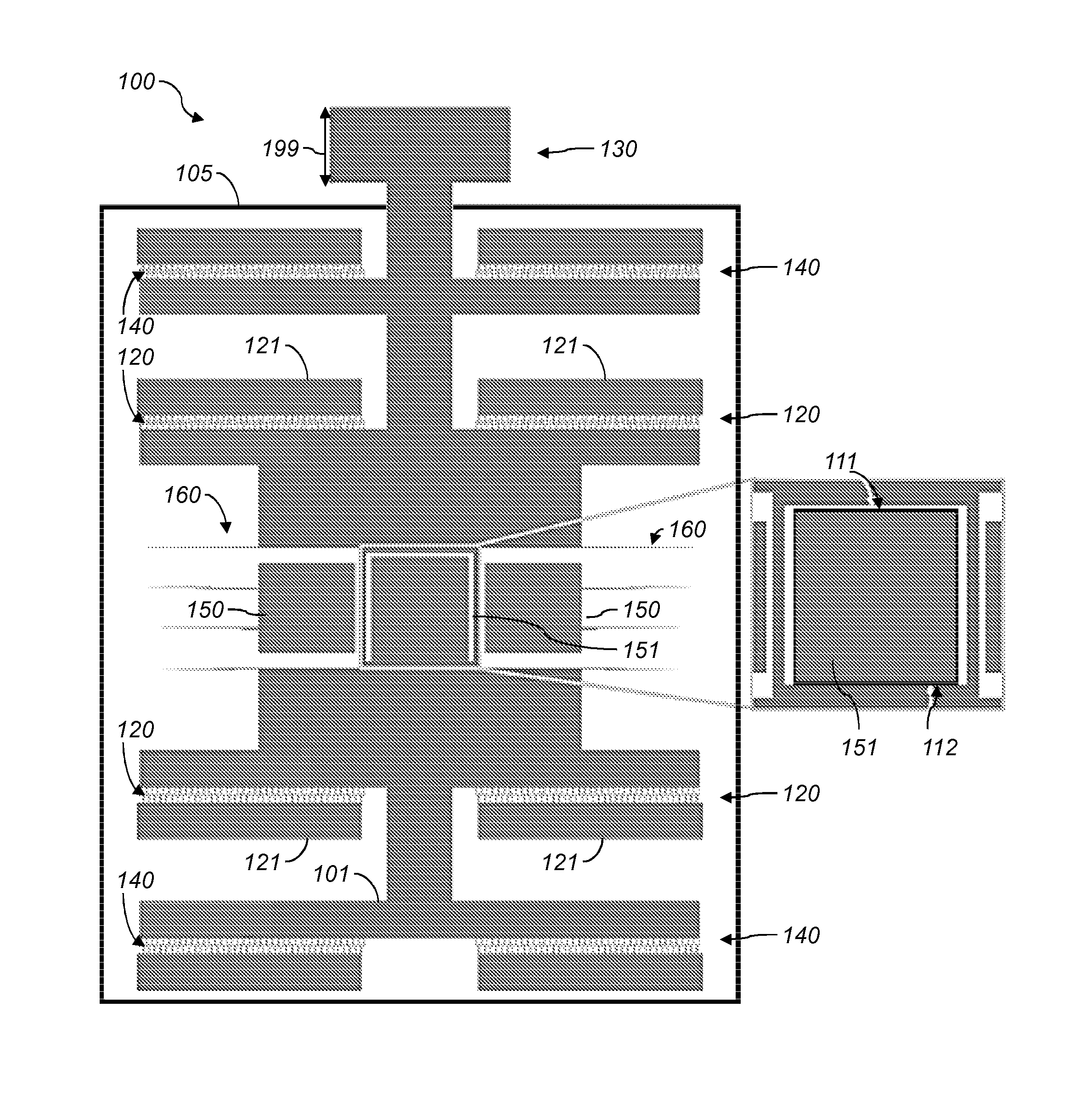
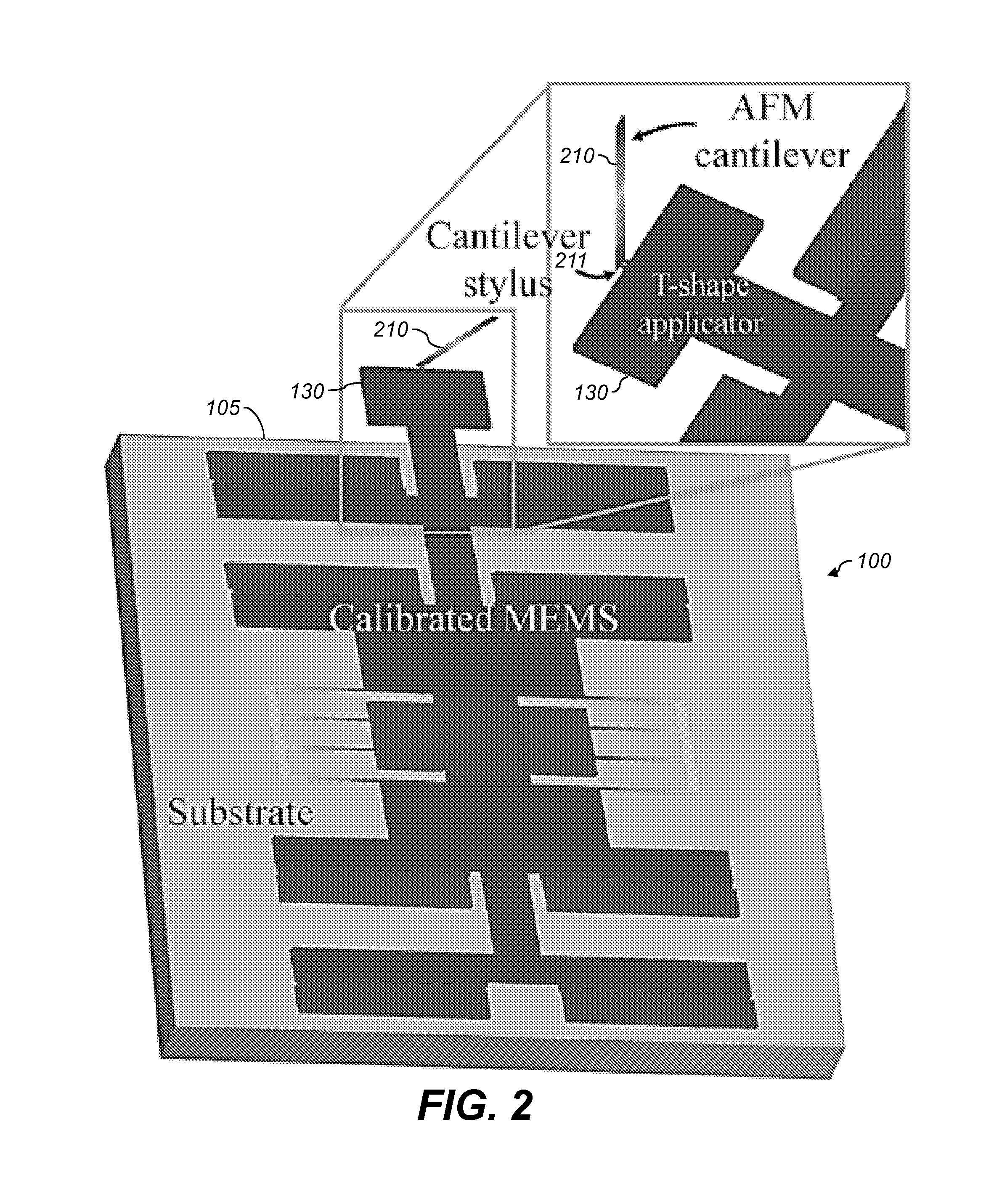
[0170]Various aspe...


PUM

PropertyMeasurementUnit
displacementaaaaaaaaaa
capacitancesaaaaaaaaaa
distanceaaaaaaaaaa

Abstract

Methods of measuring displacement of a movable mass in a microelectromechanical system (MEMS) include driving the mass against two displacement-stopping surfaces and measuring corresponding differential capacitances of sensing capacitors such as combs. A MEMS device having displacement-stopping surfaces is described. Such a MEMS device can be used in a method of measuring properties of an atomic force microscope (AFM) having a cantilever and a deflection sensor, or in a temperature sensor having a displacement-sensing unit for sensing a movable mass permitted to vibrate along a displacement axis. A motion-measuring device can include pairs of accelerometers and gyroscopes driven 90° out of phase.

Description

CROSS-REFERENCE TO RELATED APPLICATIONS[0001]This application is a nonprovisional application of, and claims priority to, U.S. Provisional Patent Applications Nos. 61 / 659,179, filed Jun. 13, 2012; 61 / 723,927, filed Nov. 8, 2012; 61 / 724,325, filed Nov. 9, 2012; 61 / 724,400, filed Nov. 9, 2012; 61 / 724,482, filed Nov. 9, 2012; and 61 / 659,068, filed Jun. 13, 2012, the entirety of each of which is incorporated herein by reference.FIELD OF THE INVENTION[0002]The present application relates to microelectromechanical systems (MEMS) and nanoelectromechanical systems (NEMS).BACKGROUND[0003]Microelectromechanical systems (MEMS) are commonly fabricated on silicon (Si) or silicon-on-insulator (SOI) wafers, much as standard integrated circuits are. However, MEMS devices include moving parts on the wafers as well as electrical components. Examples of MEMS devices include gyroscopes, accelerometers, and microphones. MEMS devices can also include actuators that move to apply force on an object. Examp...

Claims


Application Information

Patent Timeline
Patent Type & Authority Applications(United States)
IPC IPC(8): G01P15/125B81B3/00B81C99/00G01Q20/00G01K11/00
CPCG01P15/125G01Q20/00B81B3/0051B81C99/0045G01K11/00B81B2201/0235B81B2201/033B81C99/003G01C19/5755G01P15/097G01P21/00G01P2015/0871G01Q40/00
Inventor CLARK, JASON V.
Owner PURDUE RES FOUND INC
Why Eureka
Try Eureka