Insulated gate semiconductor element drive device

a technology of insulated gate semiconductor elements and drive devices, which is applied in the direction of pulse techniques, oscillation generators, power conversion systems, etc., can solve the problems of complex configuration, time-consuming and labor-intensive regulation, and the risk of causing a thermal breakdown of igbt, so as to prevent a thermal breakdown of an insulated gate semiconductor element, reduce loss and noise, and simple configuration

Active Publication Date: 2015-06-25
FUJI ELECTRIC CO LTD
View PDF3 Cites 11 Cited by
  • Summary
  • Abstract
  • Description
  • Claims
  • Application Information

AI Technical Summary

Benefits of technology

[0016]The invention, having been contrived bearing in mind these kinds of circumstances, has for its object to provide an insulated gate semiconductor element drive device, of a simple configuration, which can parallel drive a plurality of insulated gate semiconductor elements connected in parallel, uniformly and in a good current balance, with a constant current.
[0020]According to the insulated gate semiconductor element drive device of this kind of configuration, the size of a constant current, which is supplied to each of a plurality of insulated gate semiconductor elements, for turning on each of the insulated gate semiconductor elements is regulated in accordance with currents flowing through the plurality of insulated gate semiconductor elements, connected in parallel, which are individually driven by a plurality of respective drive circuits. Therefore, the turn-on times of the plurality of insulated gate semiconductor elements can be aligned regardless of variations in the gate threshold voltages of the plurality of insulated gate semiconductor elements due to the solidity of the insulated semiconductor elements. Moreover, as the constant current is supplied to each of the insulated gate semiconductor elements, each insulated gate semiconductor element can be turned on regardless of a change in on resistance of the insulated gate semiconductor elements depending on temperature. Consequently, it is possible to reduce loss and noise when the insulated gate semiconductor elements are turned on.
[0021]Therefore, according to the invention, with a simple configuration such that the size of the constant current supplied to the gates of the insulated gate semiconductor elements is regulated in accordance with the currents flowing through the insulated gate semiconductor elements, it is possible to secure the current balance of the plurality of insulated gate semiconductor elements. Therefore, according to the invention, there are virtually numerous benefits such that it is possible to prevent a thermal breakdown of an insulated gate semiconductor element due to a current concentration thereon from occurring, and the like.

Problems solved by technology

This kind of current concentration on a specific IGBT when the plurality of IGBTs 2a to 2n are turned on brings about the risk of causing a thermal breakdown of the IGBT.
Therefore, in the heretofore known technique, there is the problem that regulation requires time and effort, and in addition, the configuration is complicated.

Method used


Image

  • Insulated gate semiconductor element drive device
  • Insulated gate semiconductor element drive device
  • Insulated gate semiconductor element drive device

Examples


Embodiment Construction

[0027]Hereafter, a description will be given, referring to the drawings, of an insulated gate semiconductor element drive device according to embodiments of the invention.

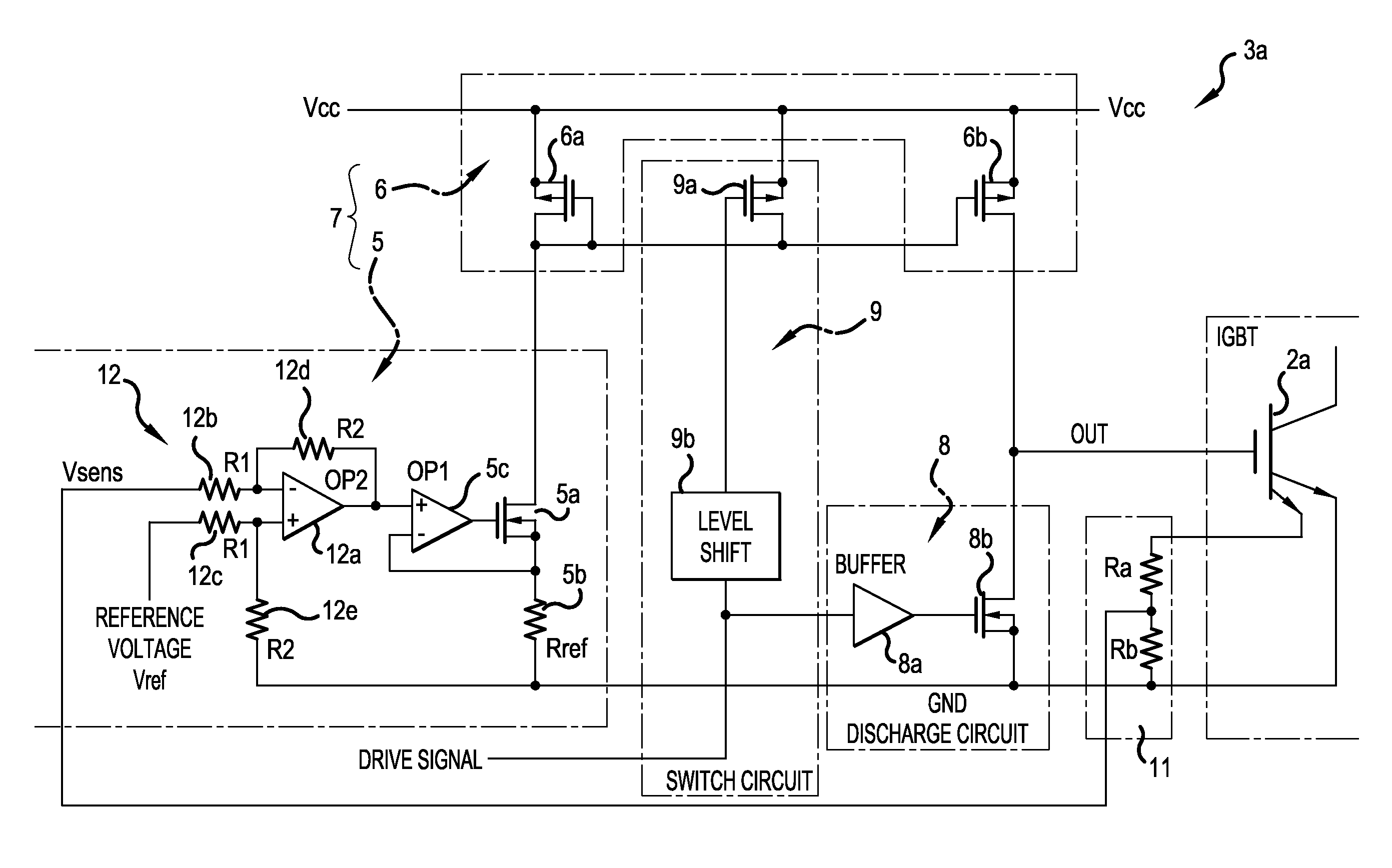
[0028]FIG. 1 is a main portion outline configuration diagram of an insulated gate semiconductor element drive device according to a first embodiment. FIG. 1 shows an outline configuration of a drive circuit 3a as a representative one of drive circuits 3a to 3n which drive a plurality of respective IGBTs 2a to 2n, but the other drive circuits 3b to 3n are configured in the same way. Also, the drive circuit 3a is shown with the same signs given to the same portions as those of a heretofore known drive circuit 3a shown in FIG. 5.

[0029]Herein, a little more detailed description will be given of the constant current circuit 7 formed of the constant current source 5 and current mirror circuit 6, the discharge circuit 8, and the switch circuit 9. The constant current source 5 is configured of an n-FET 5a, the source of wh...


PUM


Abstract

A drive circuit includes a constant current circuit which supplies a constant current to the gate of an IGBT and on-operates the IGBT; a discharge circuit which grounds the gate of the IGBT and off-operates the IGBT; and a switch circuit which operates one of the constant current circuit or discharge circuit in accordance with a control signal and turns on or off the IGBT. In particular, the drive circuit includes a current detection circuit which detects a current flowing through the IGBT when the IGBT is turned on; and a current regulation circuit which feeds the current detected by the current detection circuit back to the constant current circuit and controls an output current of the constant current circuit in accordance with the turn-on characteristics of the IGBT.

Description

CROSS-REFERENCE TO RELATED APPLICATIONS[0001]This application is a continuation of International Application No. PCT / JP 2013 / 076724, filed on Oct. 1, 2013, which is based on and claims priority to Japanese Patent Application No. JP 2012-242242, filed on Nov. 1, 2012. The disclosure of the Japanese priority application and the PCT application in their entirety, including the drawings, claims, and the specification thereof, are incorporated herein by reference.BACKGROUND OF THE INVENTION[0002]1. Technical Field[0003]The present invention relates to an insulated gate semiconductor drive device which can parallel drive a plurality of insulated gate semiconductor elements connected in parallel, uniformly, with a constant current.[0004]2. Related Art[0005]In a power converter corresponding to a large power load, a plurality of insulated gate semiconductor elements formed of IGBTs, MOS-FETs, or the like, for power control are connected in parallel, and a parallel drive of the insulated gat...

Claims


Application Information

Patent Timeline
Patent Type & Authority Applications(United States)
IPC IPC(8): H03K3/012H03K17/60
CPCH03K17/60H03K3/012H02M1/088H03K17/127
Inventor MORI, TAKAHIRO
Owner FUJI ELECTRIC CO LTD
Why Eureka
Try Eureka