Organic light emitting display device and driving method thereof

Active Publication Date: 2015-07-02
LG DISPLAY CO LTD
View PDF15 Cites 52 Cited by
  • Summary
  • Abstract
  • Description
  • Claims
  • Application Information

AI Technical Summary

Benefits of technology

[0015]Another object of the present invention is to provide an organic light emitting display device and a driving method thereof, which compensate for a driving characteristic change of a driving transistor.
[0016]Another object of the present invention is to provide an organic light emitting display device and a driving method thereof, which compensate for a threshold voltage of a driving transistor, a

Problems solved by technology

However, in the organic light emitting display device of the related art, a driving characteristic of the driving transistor Tdr may change due to non-unifor

Method used


Image

  • Organic light emitting display device and driving method thereof
  • Organic light emitting display device and driving method thereof
  • Organic light emitting display device and driving method thereof

Examples


first embodiment

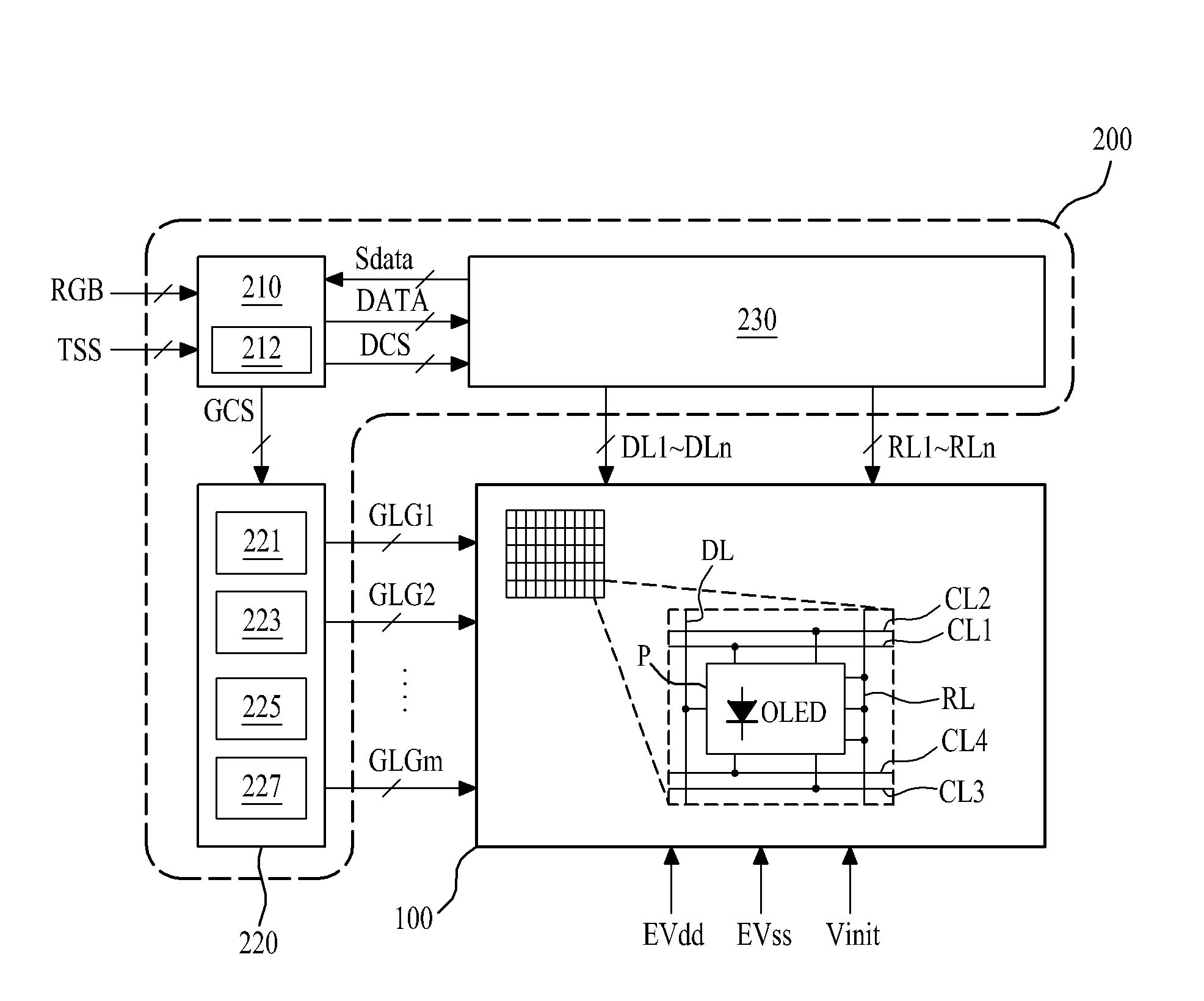
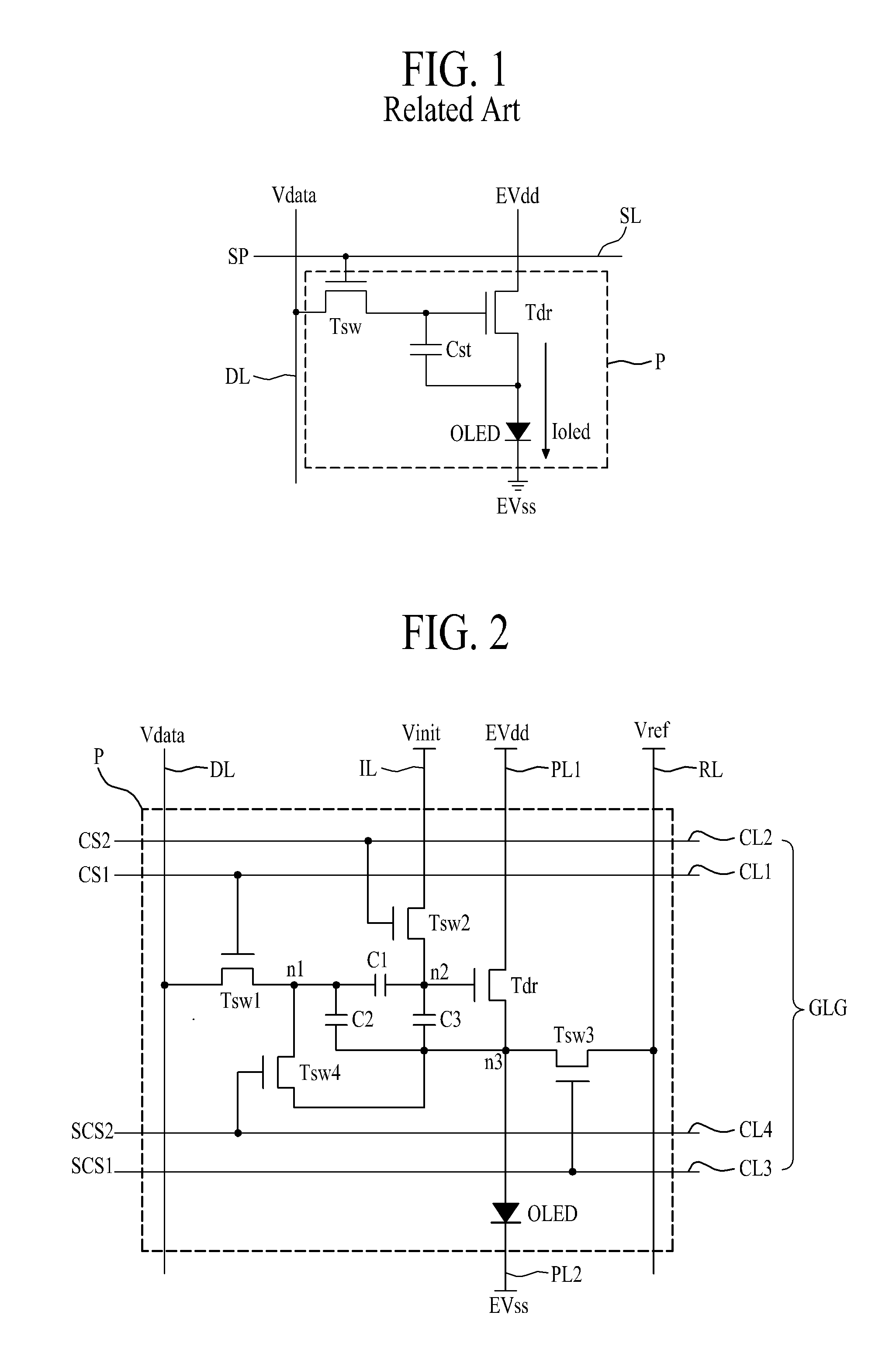
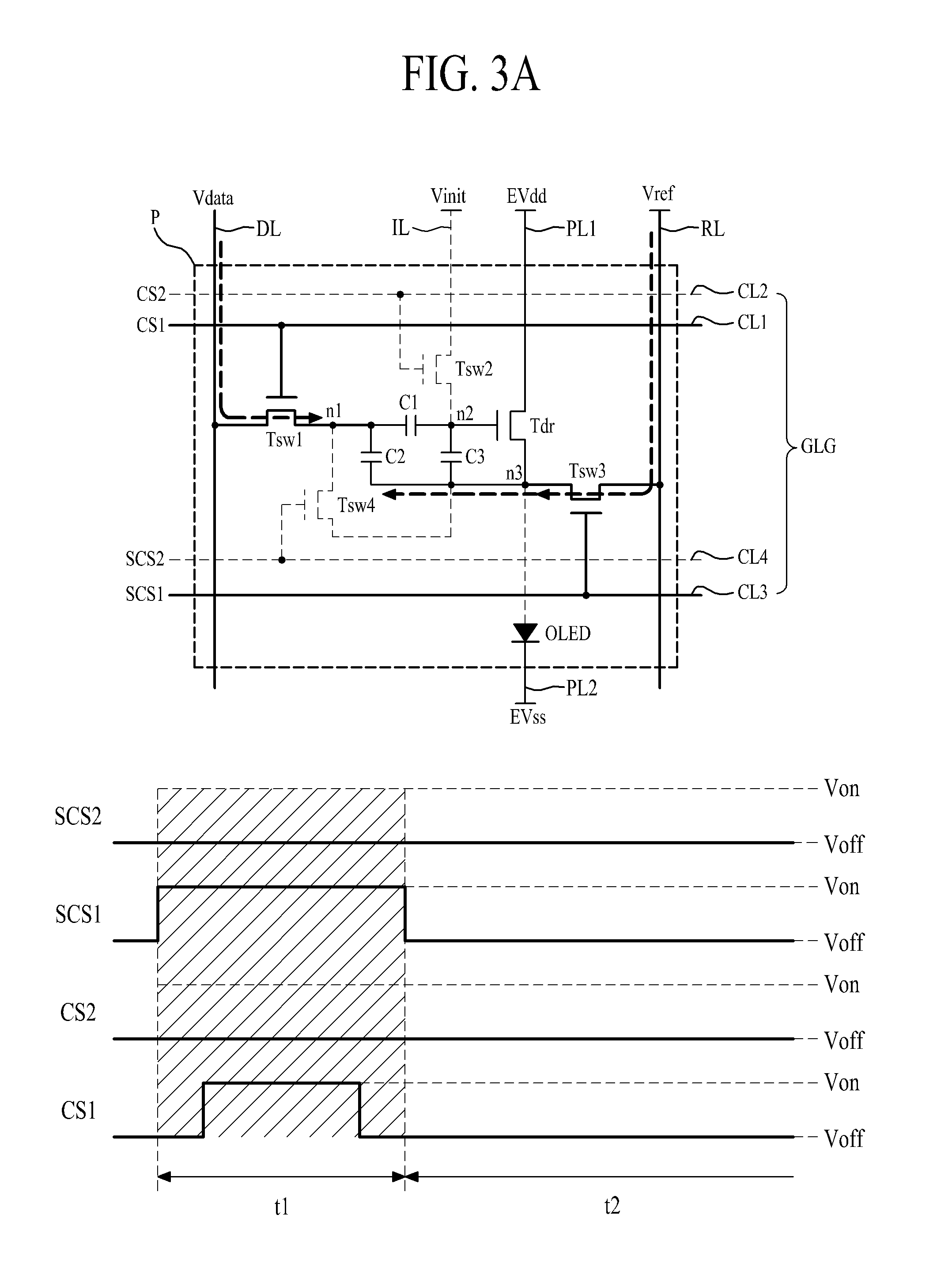
[0045]FIG. 2 is a diagram illustrating an example of a pixel structure in an organic light emitting display device. With reference to FIG. 2, a pixel P may be connected to a data line DL, a gate line group GLG, and a reference line RL. Also, the pixel P may be additionally connected to a first driving power line PL1, a second driving power line PL2, and an initial voltage line IL.

[0046]The data line DL is formed along a first direction (for example, a height direction) of a display panel (not shown). A data driver (not shown) may supply a data voltage Vdata to the data line DL.

[0047]The gate line group GLG may be formed along a second direction (for example, a width direction) of the display panel so as to intersect the data line DL. The gate line group GLG may include a scan control line CL1, an initial control line CL2, a first sensing control line CL3, and a second sensing control line CL4.

[0048]The reference line RL may be formed in parallel with the data line DL, and may be sup...

second embodiment

[0112]FIG. 7 is a diagram illustrating a pixel P structure according to an example of the present invention, which may be configured by omitting the scan control line CL1 (or the first sensing control line CL3) of the gate line group GLG. Hereinafter, only different elements may be described.

[0113]As seen in FIG. 7, in the pixel P structure according to an example of the second embodiment of the present invention, first and third switching transistors Tsw1 and Tsw3 may be simultaneously turned on or off. In detail, a first sensing control line CL3 (or the scan control line CL1) of a gate line group GLG may be connected to gate electrodes of the first and third switching transistors Tsw1 and Tsw3 in common. Therefore, the first and third switching transistors Tsw1 and Tsw3 may be simultaneously turned on or off according to a first sensing control signal SCS1 (or a scan control signal CS1) supplied to the first sensing control line CL3 (or the scan control line CL1).

[0114]As describe...

third embodiment

[0120]FIG. 8 is a diagram illustrating an example pixel structure according to the present invention, which may be configured by omitting the second sensing control line (or the initial control line) of the gate line group GLG. Hereinafter, only different elements may be described.

[0121]As seen in FIG. 8, in the pixel P structure according to an example of the third embodiment, second and fourth switching transistors Tsw2 and Tsw4 may be simultaneously turned on or off. In detail, an initial control line CL2 (or a second sensing control line CL4) of a gate line group GLG may be connected to gate electrodes of the second and fourth switching transistors Tsw2 and Tsw4 in common. Therefore, the second and fourth switching transistors Tsw2 and Tsw4 may be simultaneously turned on or off according to an initial control signal CS2 (or a second sensing control signal SCS2) supplied to the initial control line CL2 (or the second sensing control line CL4).

[0122]As described above, the pixel ...


PUM


Abstract

Disclosed is an organic light emitting display device including a pixel connected to a data line, a gate line group, and a reference line. The pixel includes an organic light emitting diode (OLED), a driving transistor configured to control a current flowing in the OLED, a first switching transistor configured to selectively supply a data voltage to a first node, a second switching transistor configured to selectively supply an initial voltage to a second node, a third switching transistor configured to selectively connect a third node to the reference line, a fourth switching transistor configured to selectively connect the first node to the third node, a first capacitor connected between the first and second nodes to store a threshold voltage of the driving transistor, and a second capacitor connected between the first and third nodes to store the data voltage supplied through the first switching transistor.

Description

CROSS-REFERENCE TO RELATED APPLICATIONS[0001]This application claims the benefit of Korean Patent Application No. 10-2013-0167896, filed on Dec. 30, 2013, which is hereby incorporated by reference as if fully set forth herein.BACKGROUND OF THE INVENTION[0002]1. Field of the Invention[0003]Embodiments of the present invention relate to an organic light emitting display device and a driving method thereof.[0004]2. Discussion of the Related Art[0005]Recently, with the advancement of multimedia, the importance of flat panel display (FPD) devices is increasing. Therefore, various FPD devices such as liquid crystal display (LCD) devices, plasma display panel (PDP) devices, and organic light emitting display devices are being used practically. The organic light emitting display devices display an image by emitting light from an organic light emitting diode according to a recombination of an electron and a positive hole. The organic light emitting display devices have a fast response time a...

Claims


Application Information

Patent Timeline
IPC IPC(8): G09G3/32
CPCG09G3/3258G09G3/3291G09G2300/0819G09G2320/043G09G2310/0208G09G2310/027G09G2320/0233G09G2300/0876G09G3/3233G09G2300/0417G09G2300/0852G09G2310/0262G09G2320/0285G09G2320/0295G09G3/32
Inventor CHANG, MIN KYUSHIM, JONG SIKTAKASUGI, SHINJI
Owner LG DISPLAY CO LTD
Why Eureka
Try Eureka