Semiconductor device

a technology of semiconductor devices and semiconductors, applied in semiconductor devices, semiconductor/solid-state device details, electrical apparatus, etc., can solve the problems of increasing temperature, preventing and the likelihood of molding resin peeling off, so as to improve the adhesion of molding resin and prevent the peeling of molding resin. , the effect of excellent anchoring

Active Publication Date: 2015-07-02
FUJI ELECTRIC CO LTD
View PDF4 Cites 17 Cited by
  • Summary
  • Abstract
  • Description
  • Claims
  • Application Information

AI Technical Summary

Benefits of technology

[0025]The semiconductor device according to the invention includes the anchor layer including the stripe-shaped concave portion which is formed in the circuit pattern formed on the front surface of the insulating plate by laser beam irradiation. Therefore, since the concave portion is filled with the molding resin, an excellent anchoring effect is obtained and the adhesion of the molding resin is improved. As a result, it is possible to prevent the molding resin from peeling off. In addition, since the surface roughness RMS of the anchor layer and the moving length of laser beam irradiation per unit area in the anchor layer are set to predetermined ranges, it is possible to effectively prevent the molding resin from peeling off.

Problems solved by technology

In addition, even though the peeling-off of the molding resin due to contraction immediately after molding is prevented, the molding resin is likely to peel off due to a difference in thermal expansion coefficient between the molding resin and the cooper material when there is a temperature variation in the usage environment of the semiconductor device 500.
Therefore, when the amount of current which flows to the external lead terminal increases, there is a concern that heat will be generated from the external lead terminal 56, resulting in an increase in temperature.
However, the effect of preventing the molding resin from peeling off is not sufficient.

Method used


Image

  • Semiconductor device
  • Semiconductor device
  • Semiconductor device

Examples


experimental example 1

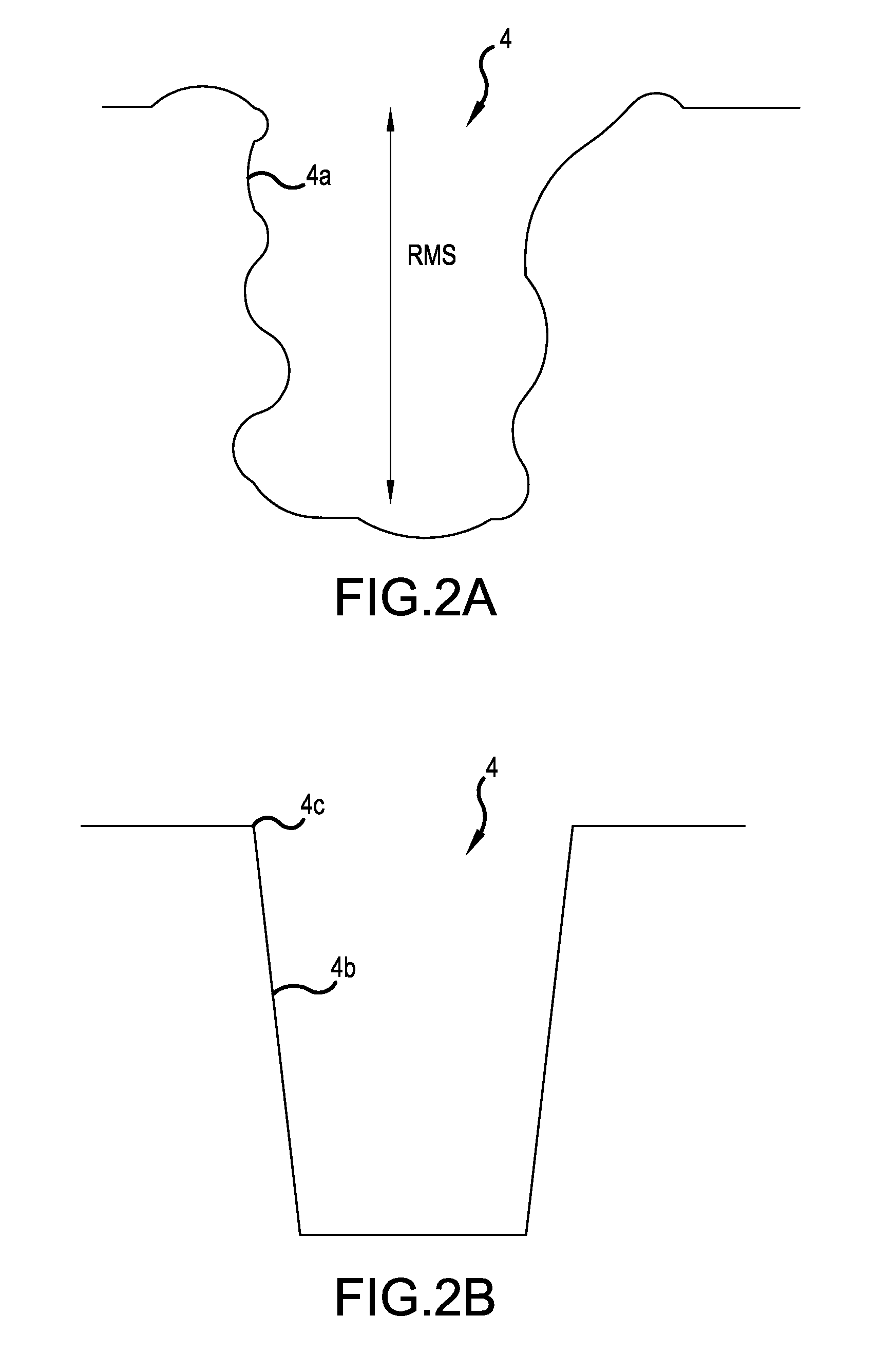
[0055]The relationship between the moving speed of laser beam irradiation and the surface roughness RMS of the anchor layer 3 formed by laser beam irradiation was investigated. Laser irradiation was performed under the conditions that a current (related to laser beam intensity) that flowed through a light source generating a laser beam was 18 A and the frequency of laser beam irradiation was 5 kHz. The concave portions 4 of the anchor layer 3 were arranged such that a pitch Q between the concave portions 4 (corresponding to the distance between laser beam irradiation positions for forming the concave portions 4) was 0.1 mm, and the width W of the anchor layer 3 was 2 mm. The surface roughness RMS was measured by a laser microscope (product name “VK-8500” manufactured by KEYENCE CORPORATION) and was measured by measuring the surface roughness of a laser irradiation area. In addition, the width of an opening of the concave portion 4 was about 0.06 mm.

[0056]When the moving speed of las...

experimental example 2

[0057]Next, experiments conducted to derive the above-mentioned Expression (1) will be described.

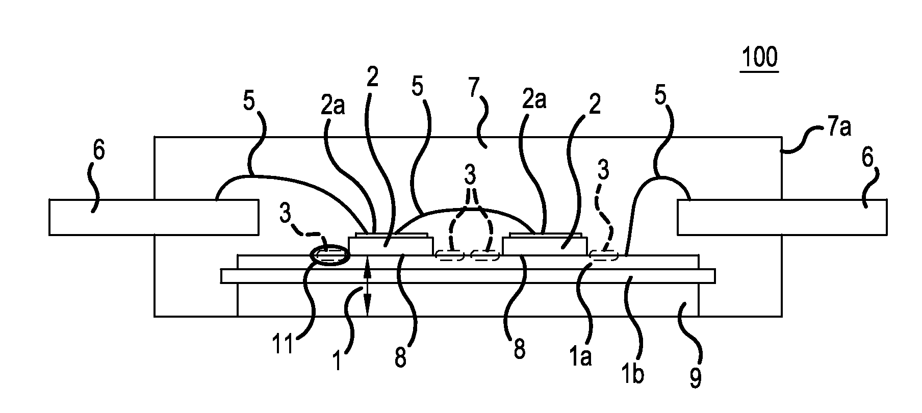
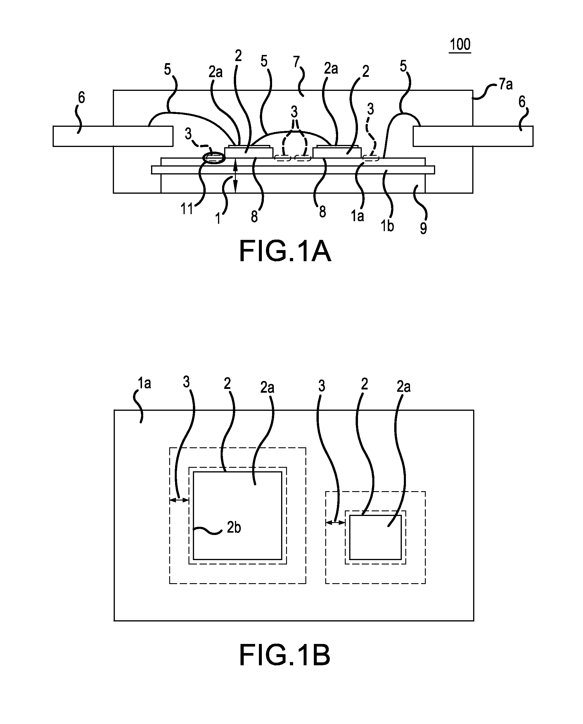
[0058]As a sample of a semiconductor device for evaluating the effect of the anchor layer 3, a semiconductor device having the same structure as that illustrated in FIG. 1 was manufactured by fixing a semiconductor chip 2 with a size of 2.5 mm×2.5 mm and a semiconductor chip 2 with a size of 1.5 mm×1.5 mm to an insulating substrate 1 with a size of about 30 mm×13 mm, connecting the insulating substrate 1 and an external lead terminal 6 with a bonding wire 5 with a diameter φ of 0.3 mm, and sealing the components with an epoxy resin which was a molding resin 7.

[0059]As the anchor layer 3, four types of samples (samples H, I, J, and K) were manufactured under the same laser irradiation conditions as those in Experimental Example 1, that is, a surface roughness RMS of 0.00175 mm to 0.0175 mm and a moving length L of laser beam irradiation per unit area of 1 mm to 10 mm. Specifically, in eac...


PUM


Abstract

A semiconductor device according to the invention includes an insulating substrate including an insulating plate, a circuit pattern that is formed on a front surface of the insulating plate, and a radiator plate that is fixed to a rear surface of the insulating plate, a semiconductor chip that is fixed to the circuit pattern, an external lead terminal that is connected to a surface electrode of the semiconductor chip through a wiring line, a molding resin that covers the insulating substrate, the semiconductor chip, the wiring line, and the external lead terminal such that a rear surface of the radiator plate and a portion of the external lead terminal are exposed, and an anchor layer including a stripe-shaped concave portion which is formed in the circuit pattern by laser beam irradiation.

Description

CROSS-REFERENCE TO RELATED APPLICATIONS[0001]This application is a continuation of International Application No. PCT / JP2013 / 083553, filed on Dec. 16, 2013, which is based on and claims priority to Japanese Patent Application No. JP 2012-277174, filed on Dec. 19, 2012. The disclosure of the Japanese priority application and the PCT application in their entirety, including the drawings, claims, and the specification thereof, are incorporated herein by reference.BACKGROUND OF THE INVENTION[0002]1. Field of the Invention[0003]The present invention relates to a semiconductor device covered with a molding resin.[0004]2. Related Art[0005]FIG. 8 illustrates a semiconductor device according to the related art. A semiconductor device 500 includes an insulating substrate 51, a semiconductor chip 52 which is fixed to an insulating substrate 51, a bonding wire 55 which has one end connected to a surface electrode 52a of the semiconductor chip 52, an external lead terminal 56 to which the other e...

Claims


Application Information

Patent Timeline
Patent Type & Authority Applications(United States)
IPC IPC(8): H01L23/31H01L23/12H01L23/522
CPCH01L23/3121H01L23/12H01L23/522H01L2224/48091H01L2224/48137H01L2924/19107H01L23/49531H01L23/49541H01L23/49548H01L23/49568H01L23/49575H01L23/24H01L2924/00014
Inventor FUKUDA, KYOHEINISHIZAWA, TATSUONISHIDA, YUHEIMOCHIZUKI, EIJI
Owner FUJI ELECTRIC CO LTD
Why Eureka
Try Eureka