
Schottky barrier diode and method of manufacturing the same

a technology of schottky barrier and diode, which is applied in the direction of basic electric elements, electrical apparatus, and semiconductor devices, can solve the problems of increasing the resistance value and increasing the on-resistance and achieves the effect of increasing the area, increasing the current quantity, and reducing the resistance of the schottky barrier diod

Active Publication Date: 2015-07-02
HYUNDAI MOTOR CO LTD
View PDF2 Cites 4 Cited by
  • Summary
  • Abstract
  • Description
  • Claims
  • Application Information

AI Technical Summary

Benefits of technology

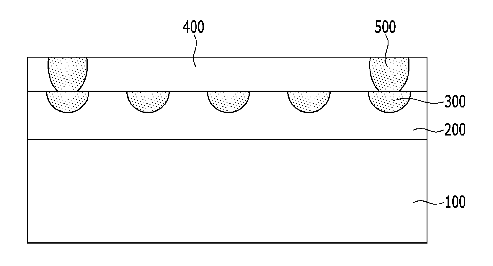
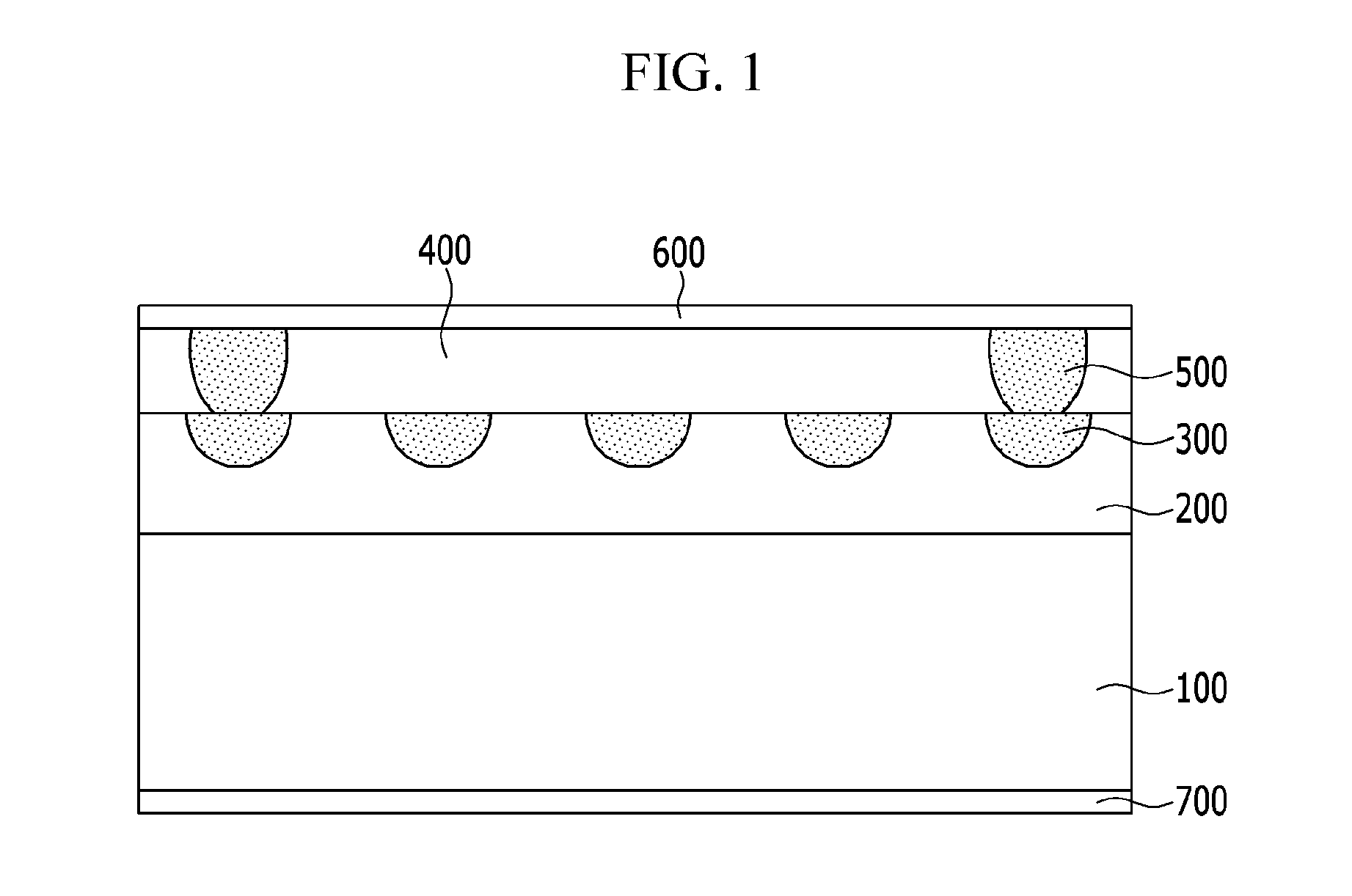
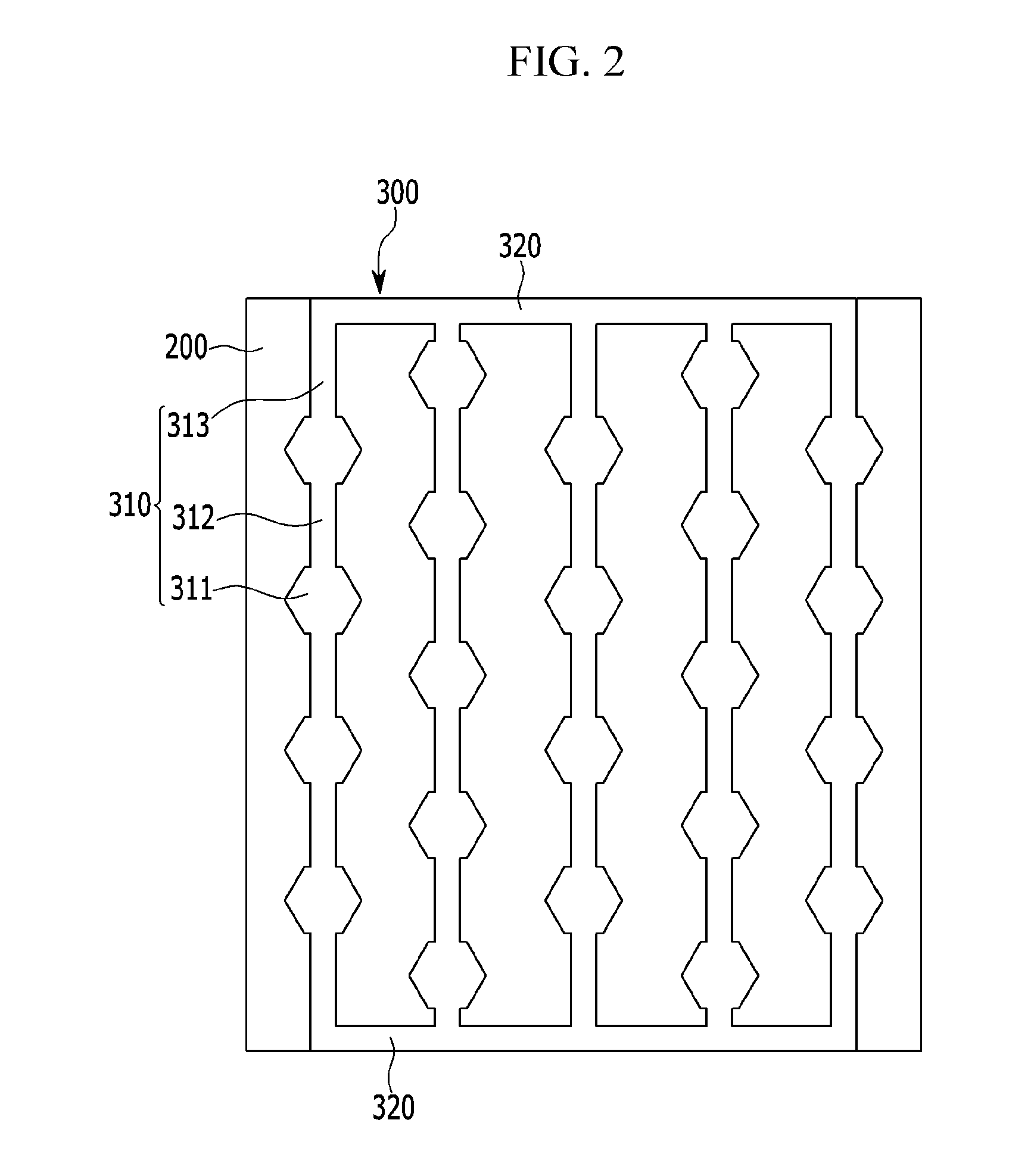
The present invention provides a Schottky barrier diode with a decreased on-resistance when a voltage is applied in a forward direction. This is achieved through a design that includes a p+ region shaped like a lattice with vertical and horizontal portions, where the vertical portion includes a first portion shaped like a hexagon to increase the area of the epitaxial layer. Additionally, the doping concentration of a contacting / Schottky electrode is higher than the doping concentration of the epitaxial layer underneath it to reduce resistance. Furthermore, the area of the Schottky junction is maximized to further reduce on-resistance when a voltage is applied in a forward direction.

Problems solved by technology

However, since the p+ region exists in the Schottky junction portion, a contact area of a Schottky electrode and an n− drift layer, which serves as a current path in a forward direction, is decreased, so that there is a problem in that a resistance value is increased, and on-resistance of the Schottky barrier diode is increased.
Further, since the p+ region floats, a width of the depletion layer blocking the leak current is not large, and thus, there is difficulty during a process of reducing an interval between the p+ regions.

Method used


Image

  • Schottky barrier diode and method of manufacturing the same
  • Schottky barrier diode and method of manufacturing the same
  • Schottky barrier diode and method of manufacturing the same

Examples


Embodiment Construction

[0028]Exemplary embodiments of the present invention will be described in detail with reference to the accompanying drawings. As those skilled in the art would realize, the described embodiments may be modified in various different ways, all without departing from the spirit or scope of the present invention. The exemplary embodiments that are disclosed herein are provided so that the disclosed contents may become thorough and complete and the spirit of the present invention may be sufficiently understood to a person of an ordinary skill in the art.

[0029]In the drawings, the thickness of layers and regions are exaggerated for clarity. In addition, in the case when it is mentioned that a layer is present “on” the other layer or a substrate, the layer may be directly formed on the other layer or the substrate or a third layer may be interposed therebetween. Like reference numerals designate like constituent elements throughout the specification.

[0030]It is understood that the term “ve...


PUM


Abstract

A Schottky barrier diode includes: an n− type epitaxial layer disposed on a first surface of an n+ type silicon carbide substrate; a first p+ region disposed on the n− type epitaxial layer; an n type epitaxial layer disposed on the n− type epitaxial layer and the first p+ region; a second p+ region disposed on the n type epitaxial layer, and being in contact with the first p+ region; a Schottky electrode disposed on the n type epitaxial layer and the second p+ region; and an ohmic electrode disposed on a second surface of the n+ type silicon carbide substrate. Also, the first p+ region has a lattice shape including a plurality of vertical portions and horizontal portions connecting both ends of the respective vertical portions to each other.

Description

CROSS-REFERENCE TO RELATED APPLICATION[0001]This application claims under 35 U.S.C. §119(a) priority to and the benefit of Korean Patent Application No. 10-2013-0167807 filed in the Korean Intellectual Property Office on Dec. 30, 2013, the entire contents of which are incorporated herein by reference.BACKGROUND[0002](a) Field of the Invention[0003]The present invention relates to a Schottky barrier diode including silicon carbide (SiC), and a method of manufacturing the same.[0004](b) Description of the Related Art[0005]A Schottky barrier diode (SBD) uses a Schottky junction in which a metal and a semiconductor are joined. The SBD, unlike a general PN diode, exhibits a rapid switching characteristic, and has a lower turn-on voltage characteristic than that of the PN diode.[0006]Generally, in a Schottky barrier diode, a structure of a junction barrier Schottky (JBS), in which a p+ region is formed at a lower end of a Schottky junction portion, is applied in order to improve a charact...

Claims


Application Information

Patent Timeline
Patent Type & Authority Applications(United States)
IPC IPC(8): H01L29/872H01L29/16H01L21/04H01L29/66
CPCH01L29/872H01L21/046H01L29/1608H01L29/6606H01L21/0495H01L29/0623H01L21/18
Inventor CHUN, DAE HWANHONG, KYOUNG-KOOKLEE, JONG SEOKPARK, JUNGHEEJUNG, YOUNGKYUN
Owner HYUNDAI MOTOR CO LTD
Learn More