Semiconductor device and method for manufacturing semiconductor device

a semiconductor and semiconductor technology, applied in the direction of semiconductor devices, electrical appliances, transistors, etc., can solve the problem of becoming increasingly difficult to introduce impurities into silicon pillars as silicon pillars become thinner, and achieve the effect of avoiding misalignmen

a semiconductor and semiconductor technology, applied in the direction of semiconductor devices, electrical appliances, transistors, etc., can solve the problem of becoming increasingly difficult to introduce impurities into silicon pillars as silicon pillars become thinner, and achieve the effect of avoiding misalignmen

US20150206923A1Inactive Publication Date: 2015-07-23UNISANTIS ELECTRONICS SINGAPORE PTE LTD

Image

  • Semiconductor device and method for manufacturing semiconductor device
  • Semiconductor device and method for manufacturing semiconductor device
  • Semiconductor device and method for manufacturing semiconductor device

Examples


Embodiment Construction

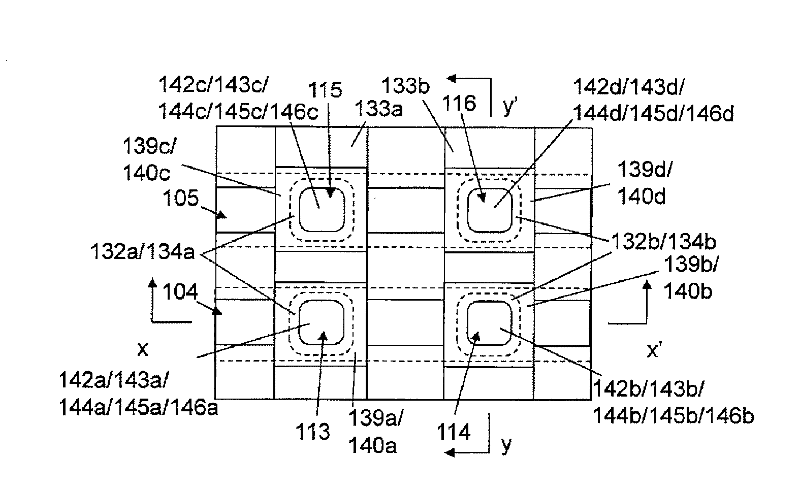
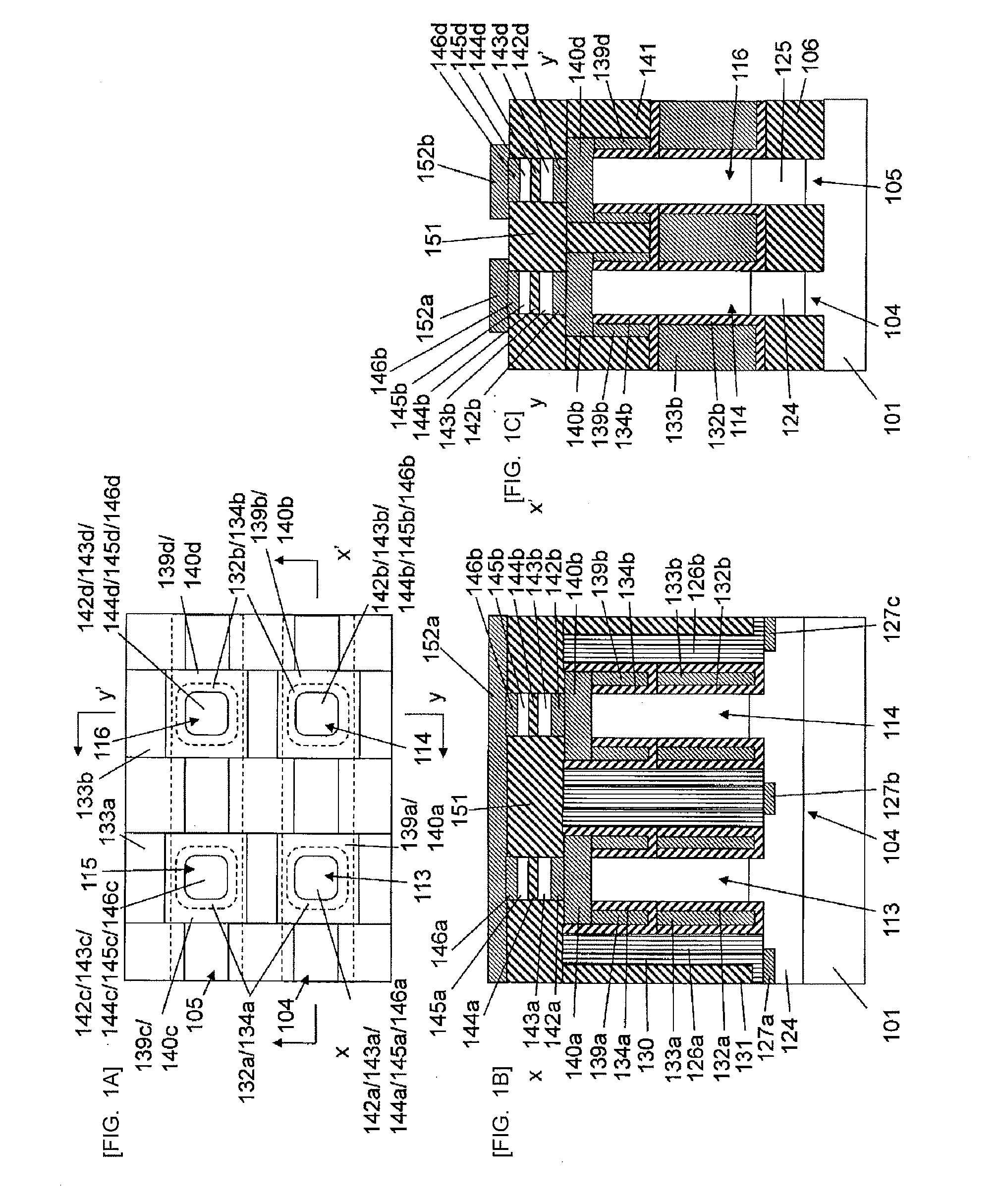
[0073]Embodiments of the present invention will now be described with reference to drawings. FIGS. 1A to 1C show a structure of a semiconductor device according to an embodiment of the present invention.

[0074]A memory cell on the lower left side of FIG. 1A includes a first fin-shaped semiconductor layer 104 disposed on a semiconductor substrate 101, a first insulating film 106 disposed around the first fin-shaped semiconductor layer 104, a first pillar-shaped semiconductor layer 113 disposed on the first fin-shaped semiconductor layer 104, a first gate insulating film 132a disposed around the first pillar-shaped semiconductor layer 113, a first gate line 133a that is disposed around the first gate insulating film 132a and extends in a direction perpendicular to the first fin-shaped semiconductor layer 104, a second diffusion layer 124 formed in a lower portion of the first pillar-shaped semiconductor layer 113, a third gate insulating film 134a surrounding an upper portion of the fi...


PUM


Abstract

A semiconductor device includes a first fin-shaped semiconductor layer on a semiconductor substrate, a first insulating film around the first fin-shaped semiconductor layer, a first pillar-shaped semiconductor layer on the first fin-shaped semiconductor layer, a first gate insulating film around the first pillar-shaped semiconductor layer, a first gate line formed around the first gate insulating film and extending in a direction perpendicular to the first fin-shaped semiconductor layer, a second diffusion layer disposed in a lower portion of the first pillar-shaped semiconductor layer, a third gate insulating film surrounding an upper portion of the first pillar-shaped semiconductor layer, a first contact electrode surrounding the third gate insulating film, a second contact electrode that connects an upper portion of the first contact electrode to an upper portion of the first pillar-shaped semiconductor layer, and a first magnetic tunnel junction memory element on the second contact electrode.

Description

RELATED APPLICATIONS[0001]This application claims priority under 35 U.S.C. ยง119 to Japanese Patent Application No. 2014-010449 filed on Jan. 23, 2014, the entire content of which is hereby incorporated by reference.BACKGROUND OF THE INVENTION[0002]1. Field of the Invention[0003]The present invention relates to a semiconductor device and a method for manufacturing a semiconductor device.[0004]2. Description of the Related Art[0005]In recent years, magnetoresistive memories have been developed (for example, see Japanese Unexamined Patent Application Publication No. 2013-93592 (hereinafter referred to as '592 document)).[0006]According to a known structure of a STT-MRAM array such as one shown in FIG. 4A of '592 document, source lines (SL) extend perpendicular to word lines (WL) and parallel to bit lines (BL). When this structure is formed by using planar transistors, an additional metal 1 is needed for source lines as shown in FIG. 4B of '592 document and thus the area used in the bit...

Claims


Application Information

Patent Timeline
23 Jul 2015
Publication
US20150206923A1
IPC
H01L27/22; H01L29/78; H01L29/66; H01L27/088
CPC
H01L21/823487; H01L27/228; H01L27/0886; H01L29/66484; H01L29/66795; H01L29/66545; H01L29/7855; H10B61/22
Inventors
MASUOKA, FUJIO; NAKAMURA, HIROKI