Delay circuit

a delay circuit and circuit technology, applied in the field of delay circuits, can solve the problems of increased cost and reduced design flexibility, and achieve the effects of simplifying the configuration of the delay circuit, reducing the influence, and increasing the design flexibility of the delay circui

Active Publication Date: 2015-07-30
FUJI ELECTRIC CO LTD
View PDF4 Cites 8 Cited by
  • Summary
  • Abstract
  • Description
  • Claims
  • Application Information

AI Technical Summary

Benefits of technology

[0009]The invention achieves the object in the foregoing by providing a delay circuit using a capacitor with an MOS structure for a delay component, which includes a clamp circuit having a first MOSFET connected to the capacitor and operating a clamp operation and a clamp release operation in response to levels of an input signal, the clamp circuit clamping a voltage applied to the capacitor to a specified charging initiation voltage at the clamp operation, a charging circuit having a first constant current source connected to the capacitor and charging the capacitor with a first constant current when the clamp operation is released, and a delayed signal producing circuit having a second MOSFET connected to the capacitor and becoming a conduction state when the voltage of the capacitor being charged reaches a voltage of a predetermined value, and a second constant current source connected to the second MOSFET, and when the second MOSFET becomes conduction, producing a delayed signal with a voltage changed by the conduction at a connection point of the second MOSFET and the second constant current source, and simultaneously discharging the capacitor with a second constant current of the second constant current source to decrease a charging speed of the capacitor.
[0013]According to the delay circuit of the invention, the circuit is capable of reducing the influence due to the voltage dependence of the capacitance of an MOS capacitor on a delay time without applying a voltage beyond the range of the power supply voltage to the MOS capacitor. Therefore, it is possible to increase the design flexibility of the delay circuit and simplify the configuration thereof.

Problems solved by technology

This requires such processing as to insulate the circuits from one another, which causes a decrease in design flexibility and an increase in complexity in the configuration of the delay circuit to result in an increased cost.

Method used


Image

  • Delay circuit
  • Delay circuit
  • Delay circuit

Examples


Embodiment Construction

[0019]In the following, an embodiment of the invention will be explained with reference to attached drawings.

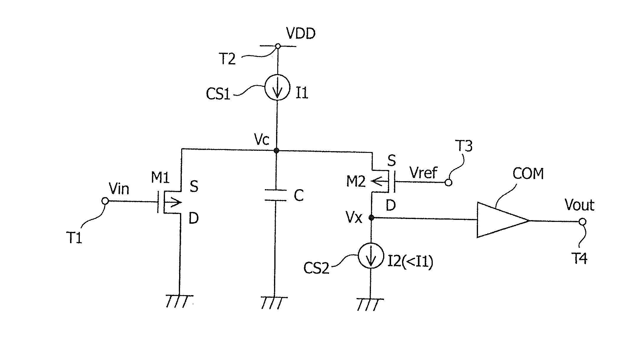
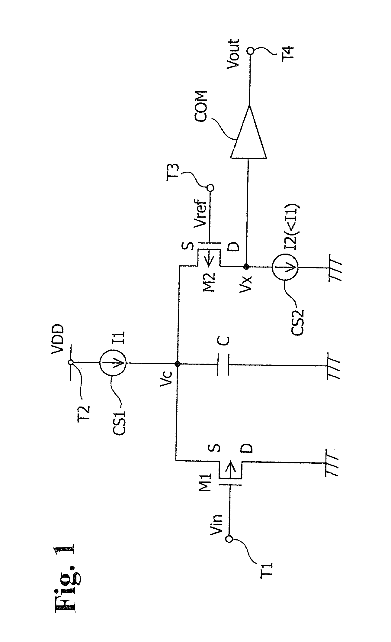
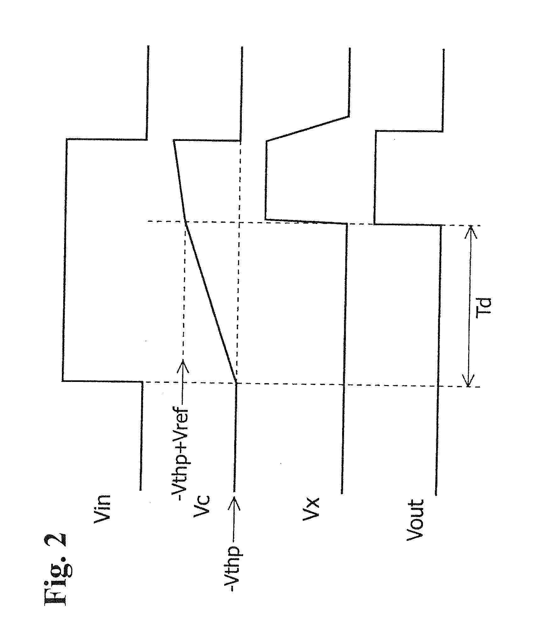
[0020]FIG. 1 is a circuit diagram showing the configuration of a delay circuit according to an embodiment of the invention. The delay circuit is provided with a first switching element M1 formed of a first MOSFET (Metal-Oxide-Semiconductor Field-Effect Transistor) and a second switching element M2 formed of a second MOSFET each being a p-channel type, first and second constant current sources CS1 and CS2 producing first and second constant currents I1 and I2 (I1>I2), respectively, a capacitor C and a voltage comparator COM. The delay circuit is formed as an integrated circuit.

[0021]The first switching element M1 has a gate terminal connected to an input terminal T1 and has a drain terminal grounded. The first constant current source CS1, being provided for forming a charging circuit charging the capacitor C with a first constant current I1, has the one end thereof connected t...


PUM


Abstract

A delay circuit using a capacitor with an MOS structure as a delay component, includes a clamp circuit operating a clamp operation and a clamp release operation in response to levels of an input signal, the clamp circuit clamping a voltage applied to the capacitor to a specified charging initiation voltage during the clamp operation; a charging circuit charging the capacitor with a constant current when the clamp operation is released; and a delayed signal producing circuit producing a delayed signal when the voltage of the capacitor being charged reaches a voltage of a predetermined value.

Description

CROSS-REFERENCE TO RELATED APPLICATION[0001]The present application claims priority from Japanese Application No. 2014-012596 filed Jan. 27, 2014, the disclosure of which is incorporated herein.FIELD OF THE INVENTION[0002]The present invention relates to a delay circuit using a capacitor as a delay element.BACKGROUND ART[0003]In JP-2001-251171, a delay circuit is disclosed which uses a capacitor with an MOS (Metal-Oxide-Semiconductor) structure (hereinafter referred to as an MOS capacitor) of a p-channel type and an MOS capacitor of an n-channel type as delay elements.[0004]As it will be explained later, an MOS capacitor has a characteristic of varying the capacitance thereof with a gate voltage (voltage dependence). Thus, when such an MOS capacitor is used as a delay element of a delay circuit, the influence on a delay time due to the voltage dependence of the MOS capacitor must be reduced.[0005]Hence, in the delay circuit according to JP-2001-251171, a specified voltage beyond the...

Claims


Application Information

Patent Timeline
Patent Type & Authority Applications(United States)
IPC IPC(8): H03K5/13
CPCH03K5/13
Inventor FUJII, MASANARI
Owner FUJI ELECTRIC CO LTD
Why Eureka
Try Eureka