INTEGRATION OF ALD BARRIER LAYER AND CVD Ru LINER FOR VOID-FREE Cu FILLING

a technology of void-free cu filling and ald barrier layer, which is applied in the direction of chemical vapor deposition coating, semiconductor/solid-state device details, coatings, etc., can solve the problems of area/cost scaling and ald barrier that have not delivered on their promise, and achieve superior cu metal filling, wide process window and design flexibility.

Active Publication Date: 2015-08-06
TOKYO ELECTRON LTD
View PDF5 Cites 5 Cited by
  • Summary
  • Abstract
  • Description
  • Claims
  • Application Information

AI Technical Summary

Benefits of technology

[0005]Embodiments of the invention provide methods for superior Cu metal filling of narrow, high-aspect-ratio recessed features used in semiconductor devices. According to an embodiment of the invention, void-free Cu metal filling is demonstrated in high aspect ratio (˜10), 20 nm wide recessed features (lines) using a processing scheme that includes a cluster tool containing various process chambers. This new integration scheme enables wide process window and design flexibility of Cu interconnects for very narrow recessed features, including recessed features with widths of 10 nm and below.

Problems solved by technology

Back-end-of-line (BEOL) performance / area / cost scaling is the foremost issue for 10 nm / 7 nm technology nodes.
However, ALD barriers have so far not delivered on their promise as PVD Ta flash deposition and / or PVD Cu seed layers were still needed to provide a good barrier-Cu interface.

Method used


Image

  • INTEGRATION OF ALD BARRIER LAYER AND CVD Ru LINER FOR VOID-FREE Cu FILLING
  • INTEGRATION OF ALD BARRIER LAYER AND CVD Ru LINER FOR VOID-FREE Cu FILLING
  • INTEGRATION OF ALD BARRIER LAYER AND CVD Ru LINER FOR VOID-FREE Cu FILLING

Examples


Embodiment Construction

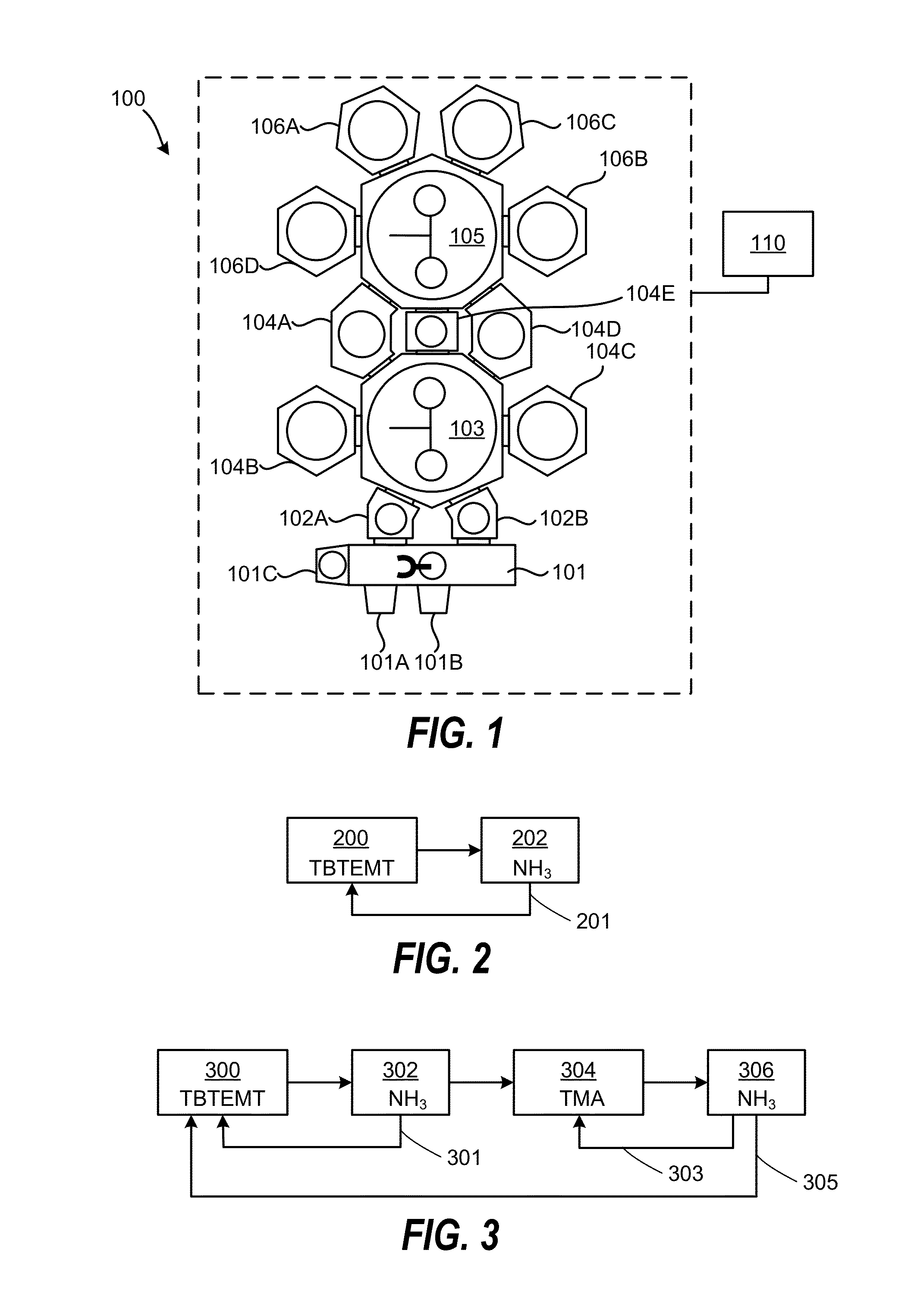
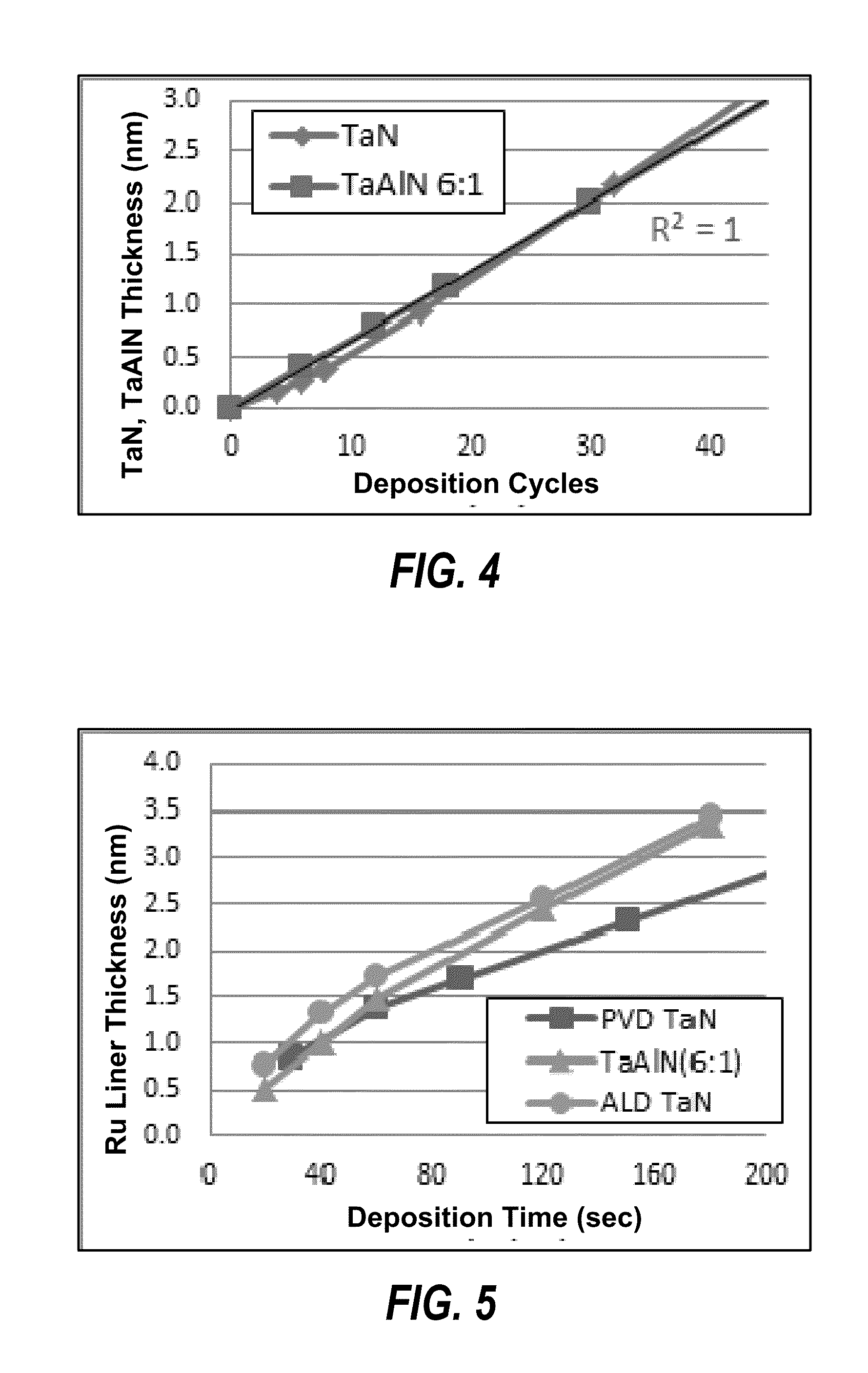
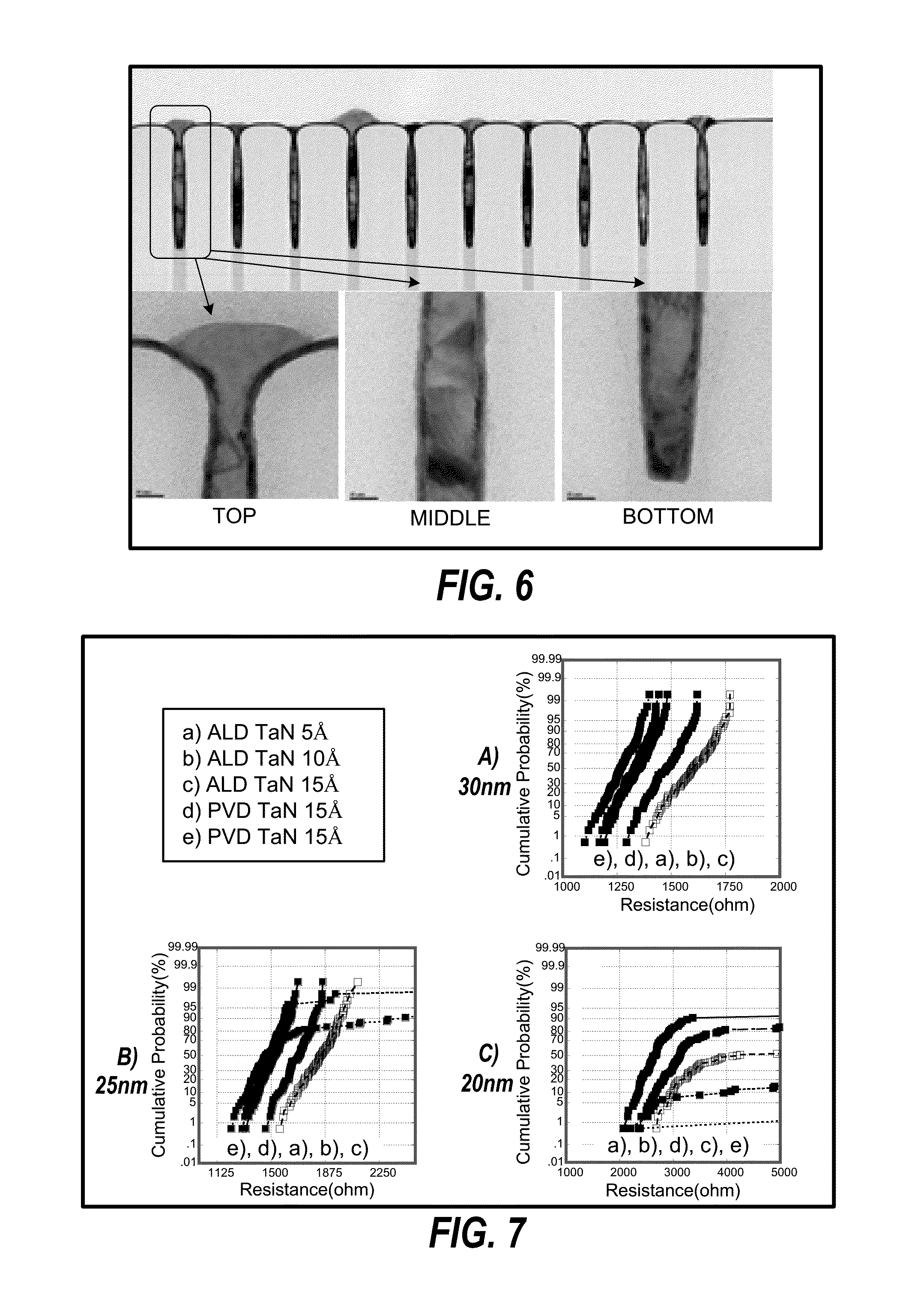
[0018]Methods for integration of ALD barrier layer and CVD Ru liner for Cu filling of narrow recessed features are disclosed in several embodiments. One skilled in the relevant art will recognize that the various embodiments may be practiced without one or more of the specific details, or with other replacement and / or additional methods, materials, or components. In other instances, well-known structures, materials, or operations are not shown or described in detail to avoid obscuring aspects of various embodiments of the invention. Similarly, for purposes of explanation, specific numbers, materials, and configurations are set forth in order to provide a thorough understanding of the invention. Furthermore, it is understood that the various embodiments shown in the drawings are illustrative representations and are not necessarily drawn to scale.

[0019]Reference throughout this specification to “one embodiment” or “an embodiment” means that a particular feature, structure, material, o...


PUM

PropertyMeasurementUnit
pressureaaaaaaaaaa
dielectric constantaaaaaaaaaa
widthaaaaaaaaaa

Abstract

Methods for integration of atomic layer deposition (ALD) of barrier layers and chemical vapor deposition (CVD) of Ru liners for Cu filling of narrow recessed features for semiconductor devices are disclosed in several embodiments. According to one embodiment, the method includes providing a substrate containing a recessed feature, depositing a conformal barrier layer by ALD in the recessed feature, where the barrier layer contains TaN or TaAlN, depositing a conformal Ru liner by CVD on the barrier layer, and filling the recessed feature with Cu metal.

Description

CROSS-REFERENCE TO RELATED APPLICATIONS[0001]This application is related to and claims priority to U.S. Provisional application Ser. No. 61 / 935,075 filed on Feb. 3, 2014, the entire contents of which are herein incorporated by reference.FIELD OF THE INVENTION[0002]The present invention generally relates to integrating conformal barriers and liners with copper (Cu) metallization in semiconductor manufacturing.BACKGROUND OF THE INVENTION[0003]Back-end-of-line (BEOL) performance / area / cost scaling is the foremost issue for 10 nm / 7 nm technology nodes. Metal lines and vias will continue to be the key areas for yield improvement, making line / via resistance as well as Cu fill the key technical challenges at 10 nm node and beyond.[0004]Physical vapor deposition (PVD) of TaN has reached its limits to meet process requirements for precise thickness and composition control, conformality, uniformity as well as interlayer dielectric damage. Atomic layer deposition (ALD) of barrier layers show pr...

Claims


Application Information

Patent Timeline
Patent Type & Authority Applications(United States)
IPC IPC(8): H01L21/768
CPCH01L21/76846H01L21/76879H01L21/76876C23C16/045C23C16/34H01L21/28562H01L21/76877H01L23/53238H01L2924/0002
Inventor YU, KAI-HUNGHASEGAWA, TOSHIOISHIZAKA, TADAHIROOIE, MANABUAMANO, FUMITAKACONSIGLIO, STEVENWAJDA, CORYMAEKAWA, KAORULEUSINK, GERT J.
Owner TOKYO ELECTRON LTD
Why Eureka
Try Eureka