Semiconductor device

Active Publication Date: 2015-08-06
TOYOTA CENT RES & DEV LAB INC
View PDF2 Cites 0 Cited by
  • Summary
  • Abstract
  • Description
  • Claims
  • Application Information

AI Technical Summary

Benefits of technology

[0009]The semiconductor device as above is characterized in that the insulated gate partially faces a portion that is to be the same potential with the source electrode so that the portion forms a capacitor. The gate-to-source parasitic capacitance depends substantially on the capacitance defined by the capacit

Problems solved by technology

It is thus difficult for the conventional semiconductor device with the gate-to-source parasitic capacitance depending on the depletion layer width to increase the gate-to-source parasi

Method used


Image

  • Semiconductor device
  • Semiconductor device
  • Semiconductor device

Examples


Example

First Embodiment

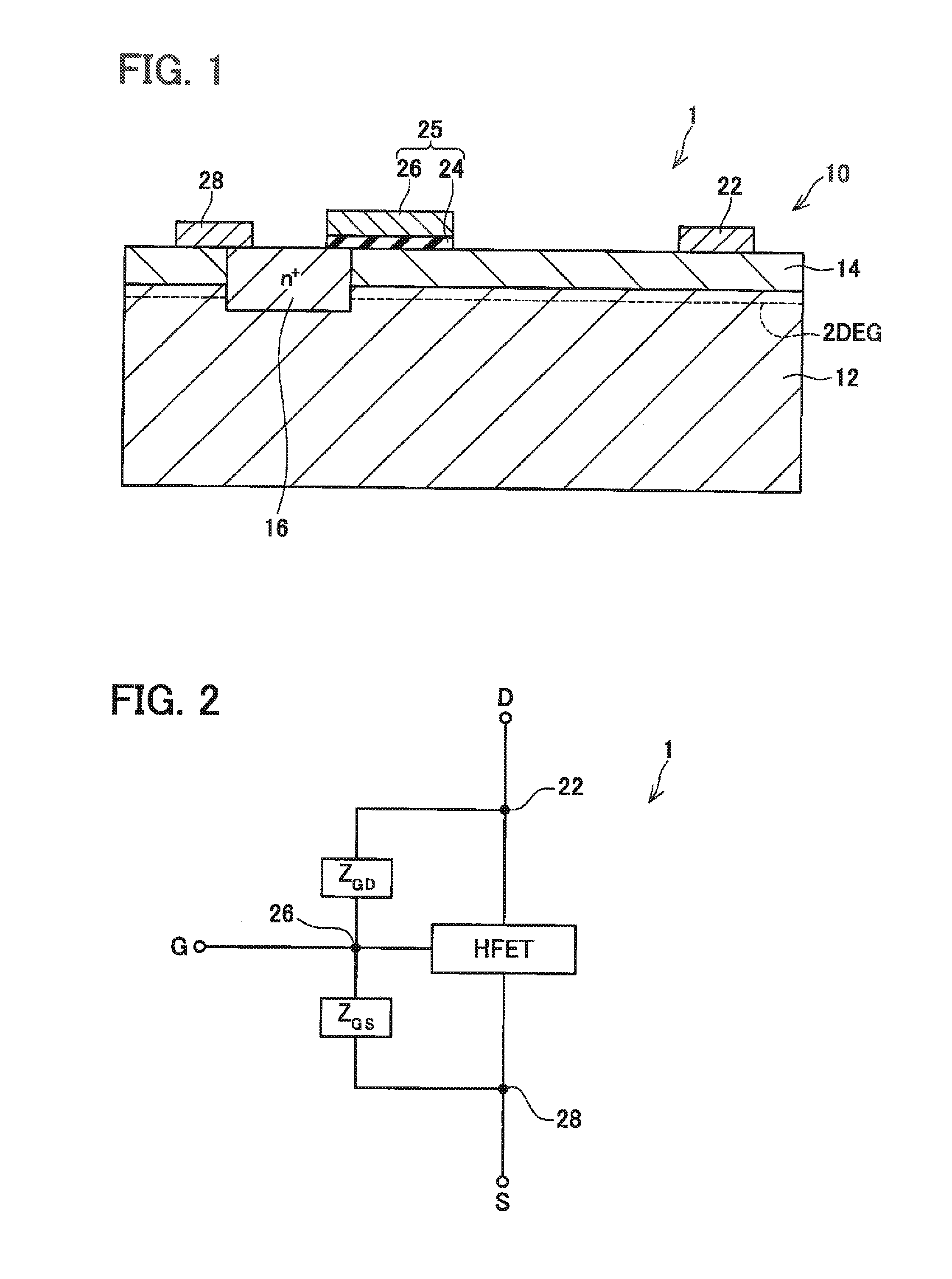
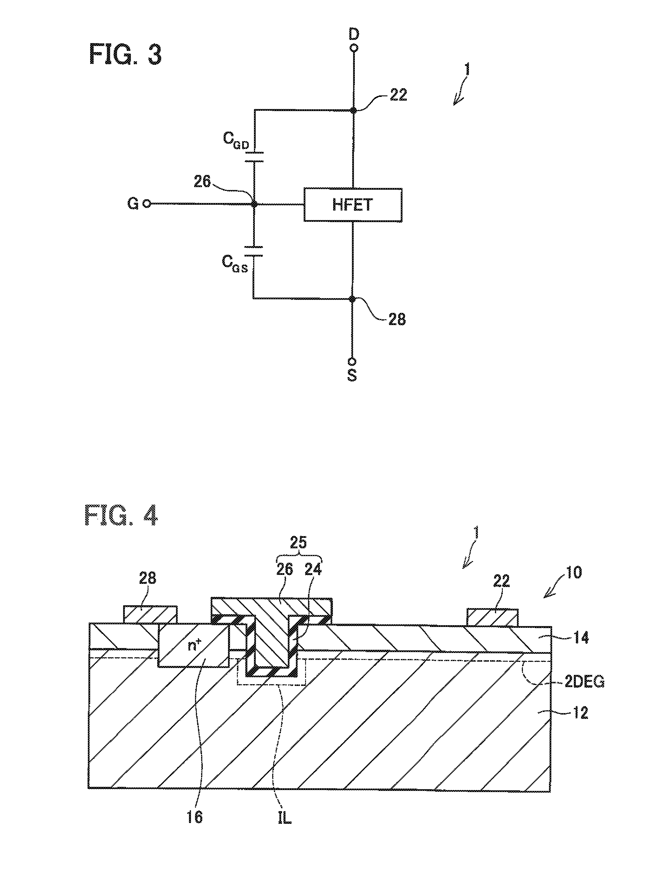
[0029]As depicted in FIG. 1, a semiconductor device 1 is of a type called HEMT (High Electron Mobility Transistor) or HFET (Heterostructure Field Effect Transistor) and includes a semiconductor laminated body 10, a drain electrode 22, an insulated gate 25, and a source electrode 28. The semiconductor laminated body 10 has an electron transit layer 12, an electron supply layer 14, and a source region 16.

[0030]Non-doped gallium nitride (GaN) is used as a material of the electron transit layer 12. The electron transit layer 12 is formed on a base substrate not shown using metal organic chemical vapor deposition (MOCVD). Notably, the electron transit layer 12 is an example of a first semiconductor layer described in Claims.

[0031]The electron supply layer 14 is disposed on the electron transit layer 12 and non-doped aluminum gallium nitride (AlGaN) is used for the material of the electron supply layer 14. Preferably, the composition ratio of aluminum in the electron suppl...

Example

Second Embodiment

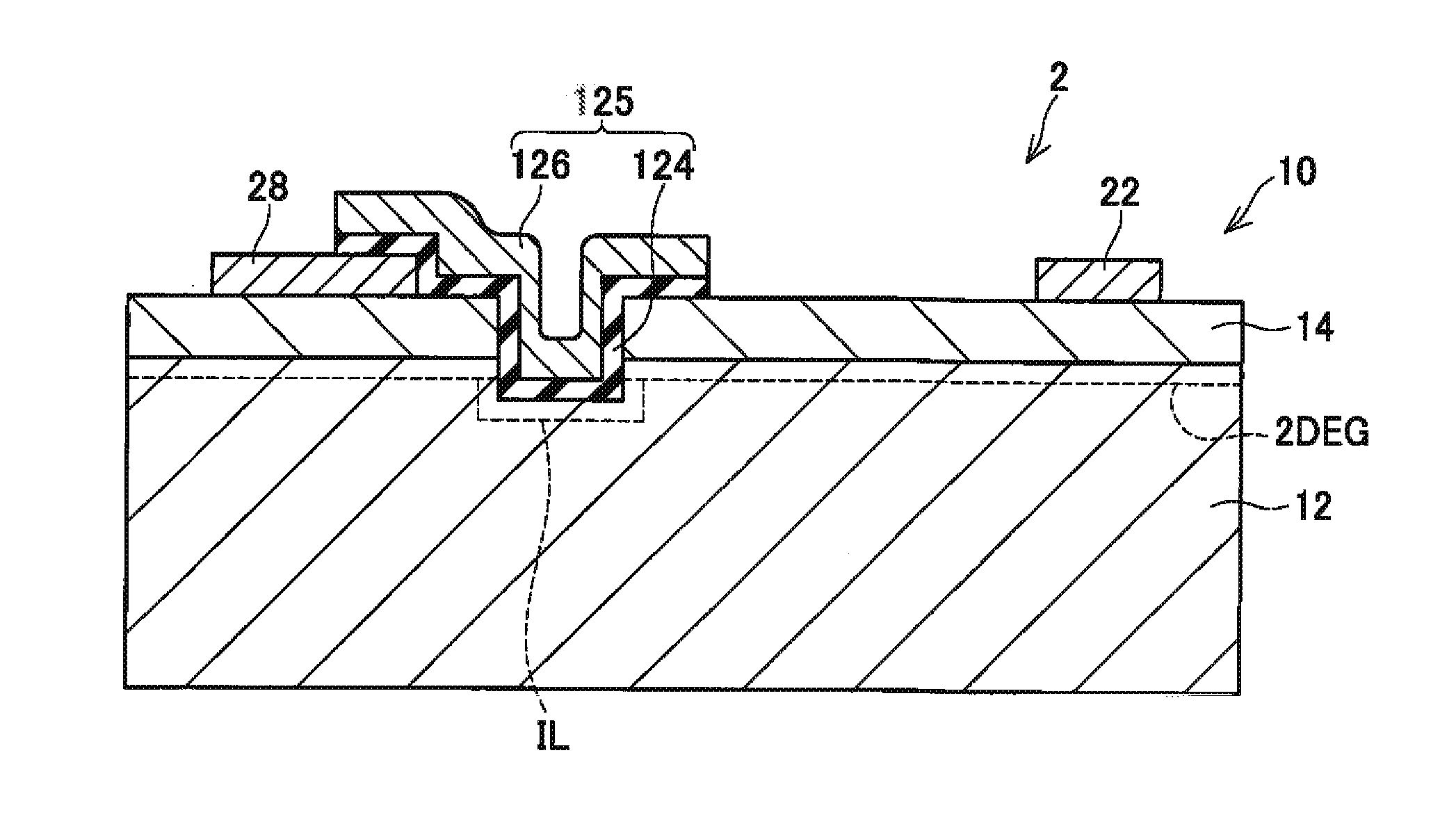
[0044]As depicted in FIG. 6, a semiconductor device 2 is characterized in that it includes an insulated gate 125 extending onto a source electrode 28. The insulated gate 125 is disposed so as to partly overlap with the source electrode 28 when viewed in plan. In the overlapping portion, a gate electrode 126 and the source electrode 28 face each other via a gate insulator film 124. Consequently, the overlapping portion forms a capacitor.

[0045]Since the semiconductor device 2 has a large capacitor capacitance as well, a relationship can be obtained where a gate-to-source parasitic capacitance CGS is relatively greater than a gate-to-drain parasitic capacitance CGD. As a result, the semiconductor device 2 also has a gate-to-source impedance ZGS be relatively smaller than a gate-to-drain impedance ZGD so that the voltage increase is suppressed at the gate electrode 126, thereby suppressing the malfunction.

[0046]As depicted in FIG. 7, the insulated gate 125 of the semico...


PUM


Abstract

A semiconductor device is provided with an electronic transit layer, an electron supply layer, a source region, a drain electrode, a source electrode and an insulated gate. In a region between the drain electrode and the insulated gate, a two-dimensional electron gas layer is configured to be generated at a hetero junction between the electronic transit layer and the electron supply layer. A part of the insulated gate is configured to face to the source region.

Description

CROSS-REFERENCE TO RELATED APPLICATION[0001]This application claims priority to Japanese Patent Application No. 2014-021142 filed on Feb. 6, 2014, the contents of which are hereby incorporated by reference into the present application.TECHNICAL FIELD[0002]The technique disclosed in the present application relates to a semiconductor device including a hetero junction.DESCRIPTION OF RELATED ART[0003]A semiconductor device that employs a two-dimensional electron gas layer formed at a hetero junction between an electron transit layer and an electron supply layer having different bandgaps, has been developed. The semiconductor device of this type is provided with a gate between a drain electrode and a source electrode so that the amount of electric current flowing between the drain electrode and the source electrode is controlled depending on voltage applied to the gate. Japanese Patent Application Publication No. 2007-96203 discloses an example of such a semiconductor device.[0004]The c...

Claims


Application Information

Patent Timeline
IPC IPC(8): H01L29/778H01L29/205H01L29/423H01L29/20
CPCH01L29/7787H01L29/2003H01L29/205H01L29/4236H01L29/0847H01L29/41775H01L29/42356H01L29/7786
Inventor UESUGI, TSUTOMUKACHI, TETSUKIKUTA, DAIGONARITA, TETSUO
Owner TOYOTA CENT RES & DEV LAB INC
Why Eureka
Try Eureka