Integrated Tunable Filter Architecture

a filter architecture and filter technology, applied in the field of electronic circuitry, can solve problems such as difficult or impossible control

Active Publication Date: 2015-08-20
PSEMI CORP
View PDF5 Cites 21 Cited by
  • Summary
  • Abstract
  • Description
  • Claims
  • Application Information

AI Technical Summary

Benefits of technology

[0030]The invention exemplified in the apparatus and method described below provides a frequency based integrated circuit solution that selectively filters out unwanted bands or regions of interfering frequencies utilizing one or more tunable notch or bandpass filters or tunable low or high pas

Problems solved by technology

Such control is difficult or impossible in many cases when a combination of integrated

Method used


Image

  • Integrated Tunable Filter Architecture
  • Integrated Tunable Filter Architecture
  • Integrated Tunable Filter Architecture

Examples


Embodiment Construction

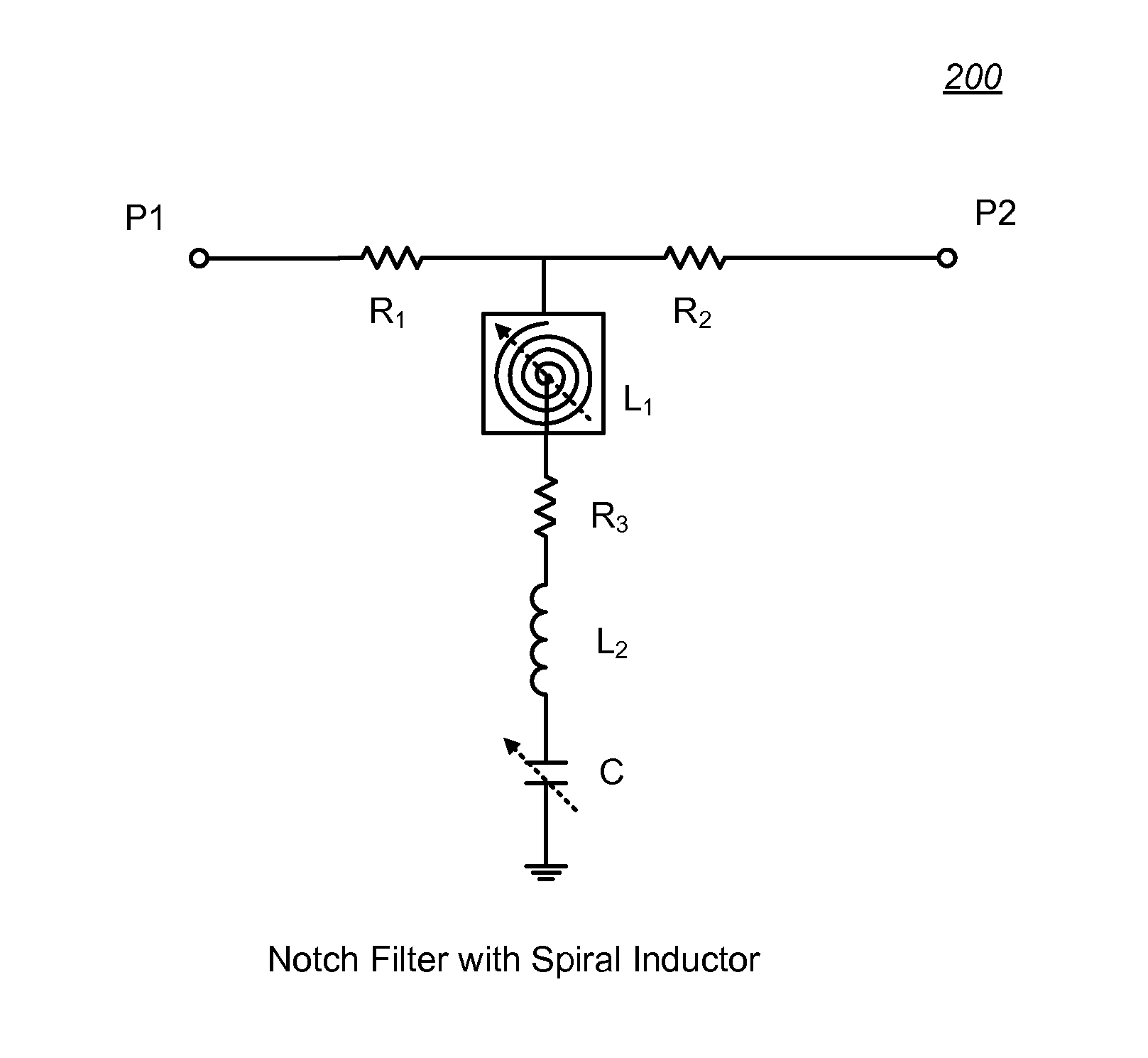
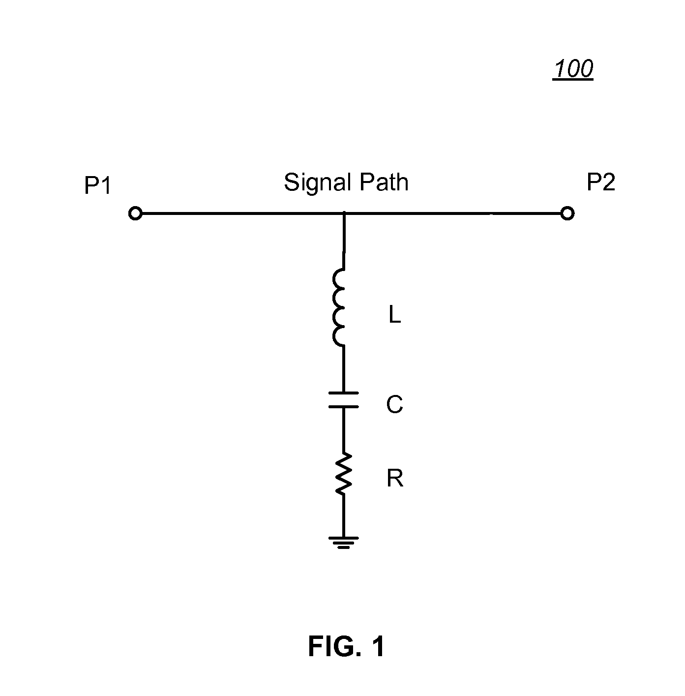
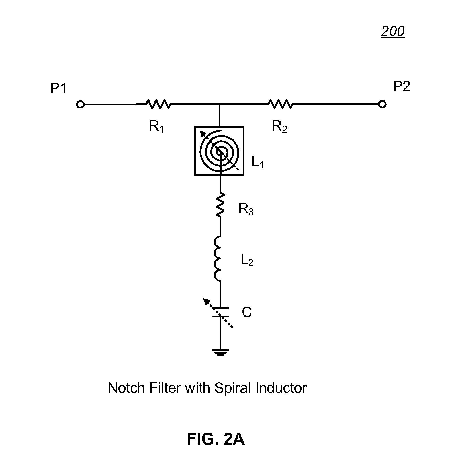
[0061]The invention exemplified in the apparatus and method described below provides a frequency based integrated circuit solution that selectively filters out unwanted bands or regions of interfering frequencies utilizing one or more tunable notch or bandpass filters or tunable low or high pass filters. The invention encompasses frequency based electronic systems or subsystems capable of operating across multiple frequencies and multiple bands in noisy environments, particularly in integrated circuit form, which is desirable from a cost, reliability, size, and low power perspective.

[0062]For RF applications in particular, it is important to carefully control all aspects of the system R, L, and C components in order to minimize their impact on signal propagation. Such control is difficult or impossible in many cases when a combination of integrated circuit (IC) circuits are combined with external R, L, and C components. Accordingly, an important aspect of the invention is that the t...


PUM

PropertyMeasurementUnit
Frequencyaaaaaaaaaa
Capacitanceaaaaaaaaaa
Insertion lossaaaaaaaaaa

Abstract

An apparatus and method for a frequency based integrated circuit that selectively filters out unwanted bands or regions of interfering frequencies utilizing one or more tunable notch or bandpass filters or tunable low or high pass filters capable of operating across multiple frequencies and multiple bands in noisy RF environments. The tunable filters are fabricated within the same integrated circuit package as the associated frequency based circuitry, thus minimizing R, L, and C parasitic values, and also allowing residual and other parasitic impedance in the associated circuitry and IC package to be absorbed and compensated.

Description

CROSS REFERENCE TO RELATED APPLICATIONS[0001]The present application may be related to the following patent applications, assigned to the assignee of the present invention, the entire disclosures of which are incorporated herein by reference:[0002](1) U.S. patent application Ser. No. 12 / 735,954, Publication No. 2011000208A1, entitled “Method and Apparatus for Use in Digitally Tuning a Capacitor in an Integrated Circuit Device”, filed on Mar. 2, 2009;[0003](2) International Application No. PCT / US2009 / 001358, entitled “Method and Apparatus for Use in Digitally Tuning a Capacitor in an Integrated Circuit Device”, filed on Mar. 2, 2009:[0004](3) U.S. patent application Ser. No. 13 / 595,893, entitled “Method and Apparatus for Use in Tuning Reactance in a Circuit Device”, filed on Aug. 27, 2012;[0005](4) U.S. patent application Ser. No. 13 / 797,779 entitled “Scalable Periphery Tunable Matching Power Amplifier”, filed on Mar. 3, 2013;[0006](5) U.S. patent application Ser. No. 13 / 797,686 enti...

Claims


Application Information

Patent Timeline
IPC IPC(8): H01L23/66H03H7/06H01L21/70H03H7/01
CPCH01L23/66H03H7/0138H03H2007/013H01L21/70H01L2223/6672H03H7/06H03H7/01H03H7/1758H03H2210/036H01L2924/0002Y10T29/4913H01L2924/00H03H7/12H03H7/0153
Inventor SMITH, WILLIAM R.ADAMSKI, JAROSLAWNOBBE, DAN WILLIAMCOMFOLTEY, EDWARD NICHOLASWANG, JINGBO
Owner PSEMI CORP
Why Eureka
Try Eureka