Transfer method for manufacturing conductor structures by means of nano-inks

a transfer method and conductor technology, applied in the direction of conductors, printed circuit non-printed electric components association, instruments, etc., can solve the problems of plastic foils, temperature susceptible to distortion, curling and in the worst case shrinkage, and restricting the possibility of producing flat conductor structures on plastic foils

Active Publication Date: 2015-08-27
GIESECKE & DEVRIENT MOBILE SECURITY GMBH
View PDF5 Cites 9 Cited by
  • Summary
  • Abstract
  • Description
  • Claims
  • Application Information

AI Technical Summary

Benefits of technology

[0041]Since with the method according to the invention there can be applied relatively high sintering temperatures, the sintering is effected within a short time span, i.e. within 30 seconds, preferably within 15 seconds, particularly preferably within 10 seconds or less. In case of particularly high-temperature-resistant transfer materials, such as Kapton, sintering times of under 5 seconds can be achieved. The very short sintering times bring along an altogether short pro

Problems solved by technology

Here, the problem arises that circuit units and foil switching elements, which are suitable for the integration into chip cards or for foil keyboards or other flat objects, normally consist of plastic foils, that is, the conductor structures must be formed on plastic foils, whereby the foils, moreover, often are thin with thicknesses in the range of about 50 μm to 300 μm.
Such plastic foils, however, at higher temperatures are susceptible to distorting, curling and in the worst case shrinking.
This property restricts the possibilities of producing flat conductor structures on plastic foils.
Ma

Method used


Image

  • Transfer method for manufacturing conductor structures by means of nano-inks
  • Transfer method for manufacturing conductor structures by means of nano-inks
  • Transfer method for manufacturing conductor structures by means of nano-inks

Examples


Embodiment Construction

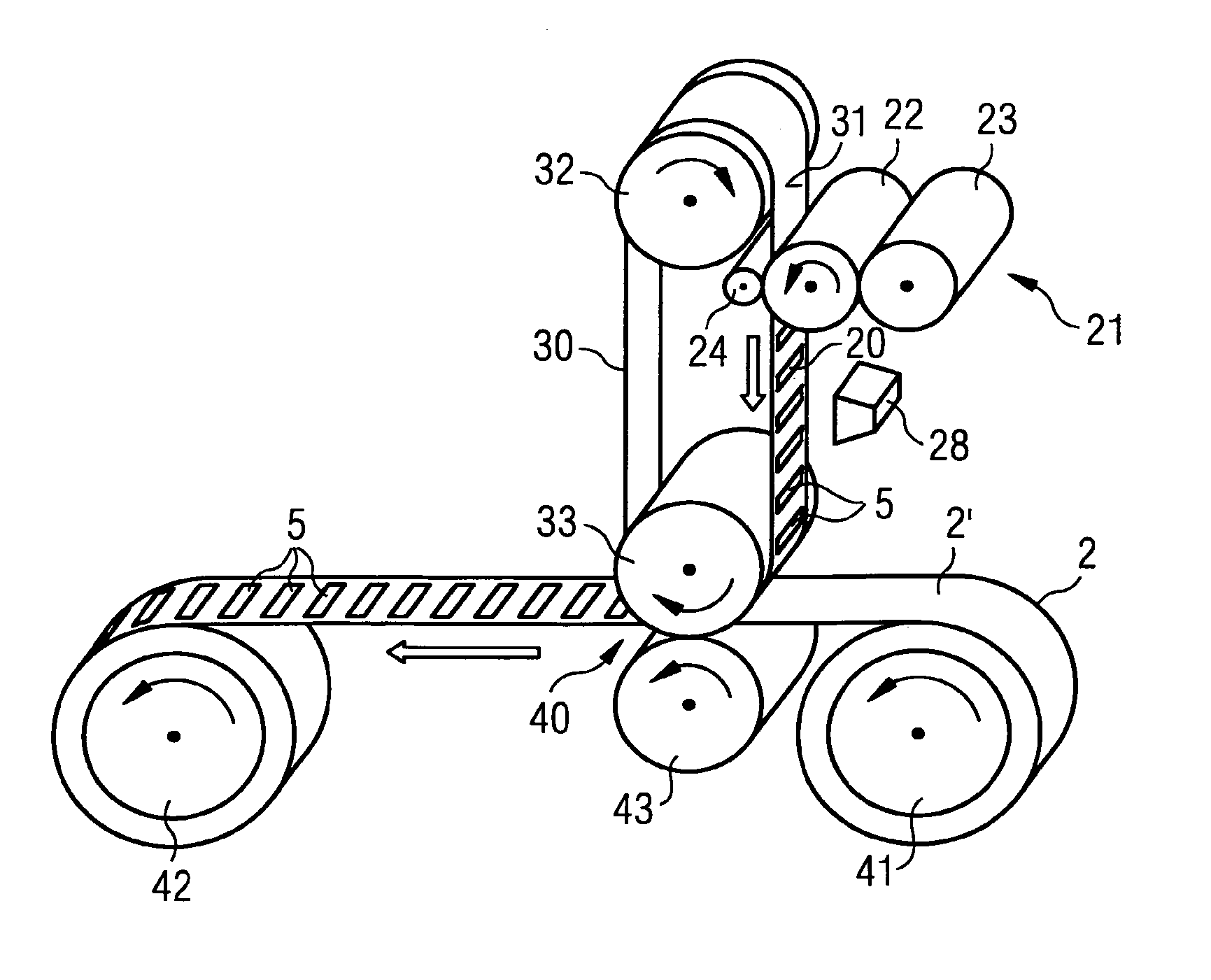
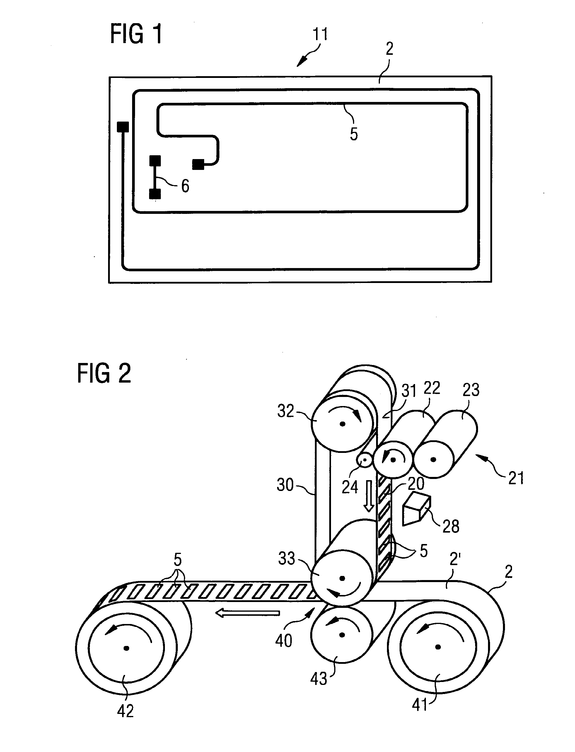
[0068]FIG. 1 shows a laminate material 11 according to the invention in a top view. The laminate material 11 has a layer made of a first foil material 2, i.e. a first foil layer 2, and a layer made of a second foil material, i.e. a second foil layer. The second foil layer is transparent and therefore not recognizable in the Figure, so that a first conductor structure 5 and a second conductor structure 6 are visible between the foil layers. The conductor structure 5 is connected with the conductor structure 6, for example the conductor structure 6 is connected with the left end of the conductor structure 5. The ends of the conductor structures 5, 6 for connection with an electronic functional element, such as an IC-chip, are respectively shown in a broadened fashion. The IC-chips themselves are omitted in the schematic representation. The first conductor structure 5 is a conductor path in the form of a coil, as is required for data carriers for the contactless data exchange or for th...


PUM

PropertyMeasurementUnit
Temperatureaaaaaaaaaa
Timeaaaaaaaaaa
Particle diameteraaaaaaaaaa

Abstract

A method for equipping a film material with at least one electrically conductive conductor structure, wherein a dispersion containing metallic nanoparticles in the form of a conductor structure is applied to a thermostable transfer material and the metallic nanoparticles are sintered to form an electrically conductive conductor structure. The electrically conductive conductor structure of sintered metallic nanoparticles is then transferred from the thermostable transfer material to the non-thermostable film material. A method for producing a laminate material using the film material using at least one electrically conductive conductor structure, and to the corresponding film material and laminate material are described.

Description

BACKGROUND OF THE INVENTION[0001]A. Field of the Invention[0002]The subject matter of the present invention is a method for equipping a foil material with at least one electrically conductive conductor structure, a method for manufacturing a laminate material which has at least two layers made of foil material and at least one electrically conductive conductor structure between the layers made of foil material, as well as foil materials manufactured by means of the method according to the invention and laminate materials having at least one electrically conductive conductor structure. Subject matter of the present invention are also products manufactured with the foil material and laminate material of the invention, such as for example security documents with electrically conductive security features, and such as electronic circuit units having IC-chip and coil for applications such as contactless data carriers in the form of flat material, as well as foil circuit elements which can...

Claims


Application Information

Patent Timeline
IPC IPC(8): B22F7/04H05K1/09B22F5/00H05K1/18B22F7/00B22F3/10
CPCB22F7/04B22F7/008H05K1/092B22F5/00H05K1/181B22F3/10G06K19/07345G06K19/07718H05K1/097H05K3/12H05K3/1275H05K3/207H05K2203/1131H05K2203/1545H01L2224/48091H01L2224/48227Y10T428/12014H01L2924/00014H01B5/00H05K3/202H05K2203/06
Inventor WELLING, ANDO
Owner GIESECKE & DEVRIENT MOBILE SECURITY GMBH
Why Eureka
Try Eureka