Thin film transistor substrate and display using the same

a technology of thin film transistors and substrates, applied in the direction of electrical equipment, semiconductor devices, instruments, etc., can solve the problem of low power consumption limitation and achieve the effect of reducing the number of mask processes and efficient manufacturing processes

Active Publication Date: 2015-08-27
LG DISPLAY CO LTD
View PDF13 Cites 21 Cited by
  • Summary
  • Abstract
  • Description
  • Claims
  • Application Information

AI Technical Summary

Benefits of technology

[0011]Another object of the present invention is to provide a thin film transistor substrate for a flat panel display having

Problems solved by technology

However, using already developed technologies, a limitati

Method used


Image

  • Thin film transistor substrate and display using the same
  • Thin film transistor substrate and display using the same
  • Thin film transistor substrate and display using the same

Examples


first embodiment

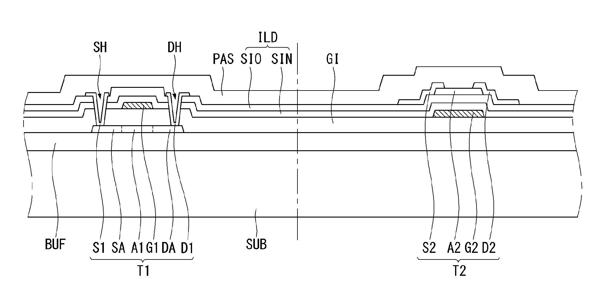
[0037]FIG. 1 is a cross sectional view illustrating a structure of a thin film transistor substrate for a flat panel display in which two different type thin film transistors are formed according to the present disclosure. Here, the cross sectional views more clearly and conveniently show the main features of the present disclosure.

[0038]With reference to FIG. 1, the thin film transistor substrate for a flat panel display according to the first embodiment comprises a first thin film transistor T1 and a second thin film transistor T2 which are disposed on the same substrate SUB. The first and second thin film transistors T1 and T2 may be far apart from each other, or they may be disposed within a relatively close distance. Otherwise, these two thin film transistors are disposed as being overlapping each other.

[0039]On the whole surface of the substrate SUB, a buffer layer BUF is deposited. In some cases, the buffer layer BUF may not be included. Or, the buffer layer BUF may be a plur...

second embodiment

[0069]FIG. 3 is a cross sectional view illustrating a structure of a thin film transistor substrate for a flat panel display in which two different types of thin film transistors are formed according to the present disclosure.

[0070]The thin film transistor substrate according to the second embodiment is basically very similar to that of the first embodiment. The main difference is on the intermediate layer ILD includes three layers. Especially, the intermediate layer ILD includes a lower oxide layer SIO1, a nitride layer SIN and an upper oxide layer SIO2, stacked sequentially.

[0071]The intermediate layer ILD also acts as a gate insulating layer for the second thin film transistor T2. Therefore, when the intermediate layer ILD is too thick, the gate voltage many not be properly applied to the second semiconductor layer A2. Therefore, the whole thickness of the intermediate layer ILD preferably has a thickness of 2,000 Å-6,000 Å.

[0072]By the post-thermal process, the hydrogen particle...


PUM


Abstract

The present disclosure relates to a thin film transistor substrate having two different types of thin film transistors on the same substrate. A thin film transistor substrate includes a substrate; a first thin film transistor disposed on the substrate, the first thin film transistor including a poly crystalline semiconductor layer, a first gate electrode over the poly crystalline semiconductor layer, a first source electrode, and a first drain electrode; a second thin film transistor disposed on the substrate, the second thin film transistor including a second gate electrode, an oxide semiconductor layer over the second gate electrode, a second source electrode, and a second drain electrode; and an intermediate insulating layer including a nitride layer and an oxide layer on the nitride layer, the intermediate insulating layer disposed over the first gate electrode and the second gate electrode and under the oxide semiconductor layer.

Description

[0001]This application claims the benefit of U.S. Provisional App. No. 61 / 943,628, filed on Feb. 24, 2014, which is incorporated herein by reference for all purposes as if fully set forth herein.BACKGROUND OF THE INVENTION[0002]1. Field of the Invention[0003]The present disclosure relates to a thin film transistor substrate having two different types of thin film transistors on the same substrate, and a display using the same.[0004]2. Discussion of the Related Art[0005]Nowadays, as the information society is developed, the requirements of displays for representing information are increasing. Accordingly, various flat panel displays (or ‘FPD’) are developed for overcoming many drawbacks of the cathode ray tube (or ‘CRT’) such as heavy weight and bulk volume. Flat panel display devices include a liquid crystal display device (or ‘LCD’), a plasma display panel (or ‘PDP’), a organic light emitting display device (or ‘OLED’) and a electrophoresis display device (or ‘ED’).[0006]The displa...

Claims


Application Information

Patent Timeline
IPC IPC(8): H01L27/12H01L29/786H01L27/32H01L29/04
CPCH01L27/1251H01L29/04H01L27/1248H01L27/3244H01L29/78675H01L29/7869G02F1/13624G02F1/1368H01L27/1225G02F1/13685H01L29/78645H01L29/78696H01L27/1214H01L21/8221H10K59/12
Inventor LEE, YOUNGJANGSON, KYUNGMOLEE, SOHYUNGPARK, MOONHOLEE, SUNGJIN
Owner LG DISPLAY CO LTD
Why Eureka
Try Eureka