Organic light emitting display device

a technology of organic light and display device, which is applied in the direction of thermoelectric device junction materials, semiconductor devices, electrical apparatus, etc., can solve the problems of difficult to manufacture high-resolution or high-transparent panels, limit the size of thin-film transistors, capacitors and various types of supply lines required for driving oled devices, etc., and achieves high aperture ratio, high resolution, and easy driving

Active Publication Date: 2015-08-27
LG DISPLAY CO LTD
View PDF0 Cites 93 Cited by
  • Summary
  • Abstract
  • Description
  • Claims
  • Application Information

AI Technical Summary

Benefits of technology

[0034]According to the present invention, a pixel and another pixel adjacent to the pixel have a gate line in common, so that it is possible to provide an OLED device with high aperture ratio and high resolution.
[0035]Further, according to the present invention, an OLED device can be more easily driven by forming driving thin-film transistors, such as an oxide semiconductor thin-film transistor and an LTPS thin-film transistor respectively, in adjacent pixels sharing a gate line,
[0036]In addition, according to the present invention, by fo

Problems solved by technology

However, there are limits to reduce the sizes of thin-film transistors, capacitors and various types of supply lines

Method used


Image

  • Organic light emitting display device
  • Organic light emitting display device
  • Organic light emitting display device

Examples


Embodiment Construction

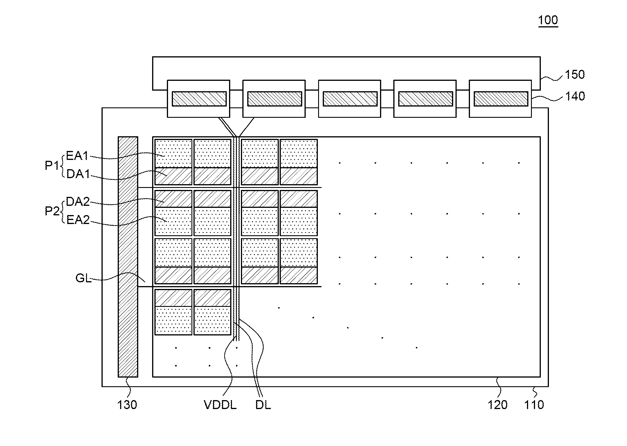
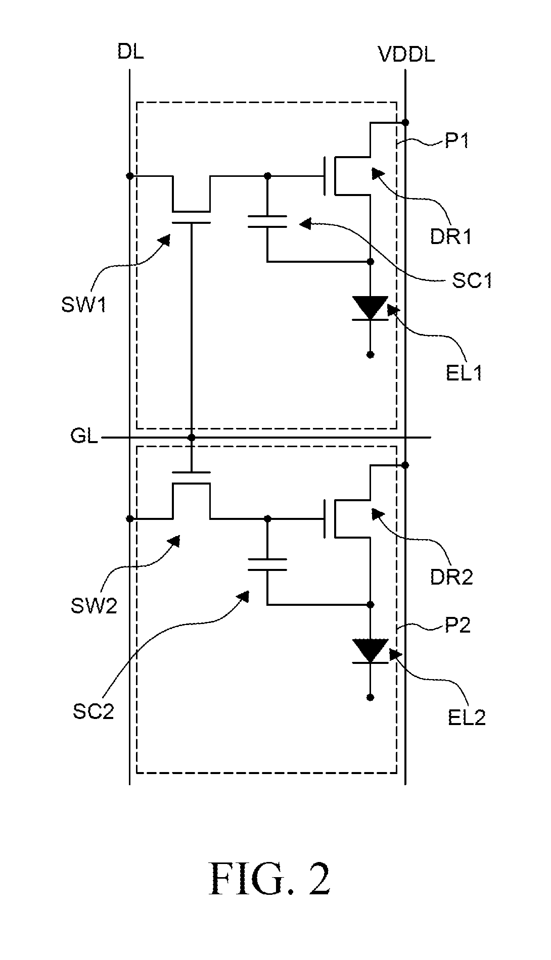
[0047]Advantages and features of the present invention and methods to achieve them will become apparent from the descriptions of exemplary embodiments herein below with reference to the accompanying drawings. However, the present invention is not limited to exemplary embodiments disclosed herein but may be implemented in various different ways. The exemplary embodiments are provided for making the disclosure of the present invention thorough and for fully conveying the scope of the present invention to those skilled in the art. It is to be noted that the scope of the present invention is defined only by the claims.

[0048]The figures, dimensions, ratios, angles, numbers of elements given in the drawings are merely illustrative and are not limiting. Like reference numerals denote like elements throughout the descriptions. Further, in describing the present invention, descriptions on well-known technologies may be omitted in order not to obscure the gist of the present invention. It is ...


PUM


Abstract

Disclosed herein is an OLED (Organic Light Emitting Display) device. A switching thin-film transistor configured to be an oxide semiconductor thin-film transistor is disposed in a first pixel. A second pixel is adjacent to the first pixel in the direction in which data lines are extended. A switching thin-film transistor configured to be an LTPS (Low Temperature Poly-Silicon) thin-film transistor is disposed in the second pixel. The switching thin-film transistor of the first pixel and the switching thin-film transistor of the second pixel are connected to the same gate line. A pixel and another pixel adjacent to the pixel connected to a gate line in common, so that it is possible to provide an OLED device with high aperture ratio and high resolution.

Description

CROSS-REFERENCE TO RELATED APPLICATIONS[0001]This application claims the priority under 35 U.S.C. §119(e) to U.S. Provisional Application No. 61 / 944,499 filed on Feb. 25, 2014, and under 35 U.S.C. §119(a) to Korean Patent Application No. 10-2014-0097125 filed on Jul. 30, 2014, which are incorporated by reference herein in their entirety.BACKGROUND OF THE INVENTION[0002]1. Field of the Invention[0003]The present invention relates to an OLED (Organic Light Emitting Display) device. More particularly, the present invention relates to an OLED device achieving high aperture ratio and being advantageously applied to high resolution devices, in which an oxide semiconductor thin-film transistor having an active layer made of an oxide semiconductor and an LTPS (Low Temperature Poly-Silicon) thin-film transistor having an active layer made of an low temperature poly-silicon are supplied with the same gate voltage from the same gate line. Further, the present invention relates to an OLED devic...

Claims


Application Information

Patent Timeline
IPC IPC(8): H01L27/32
CPCH01L27/3262H01L27/3248H01L27/3272H01L27/3265H01L27/3276H01L27/1255H01L27/1251H01L27/1225H10K59/121H10K59/1213H10K59/1216H10K59/131H10K59/123H10K59/126H01L29/78675H01L29/7869
Inventor KWON, HOI YONGLEE, JOON SUKKIM, EUI TAEPARK, SUNG HEESHIN, KI SEOB
Owner LG DISPLAY CO LTD
Why Eureka
Try Eureka