Stacked Die Flash Memory Device With Serial Peripheral Interface

a flash memory device and serial peripheral technology, applied in the field of flash memory, can solve the problems of high cost, inability to operate flash memory devices with stacked spi flash memory devices, and inability to meet the requirements of high density monolithic silicon dies, and achieve the effect of increasing capacity

Active Publication Date: 2015-09-03
WINBOND ELECTRONICS CORP
View PDF2 Cites 17 Cited by
  • Summary
  • Abstract
  • Description
  • Claims
  • Application Information

AI Technical Summary

Problems solved by technology

Monolithic silicon die at high density is feasible but costly.
The techniques to operate a flash memory device having stacked SPI flash memory die are not entirely satisfactory.
Disadvantageously, the controller is required to provide and manage multiple / CS control signals.
While such a device can operate with a Quad I / O SPI protocol in an 8-pin package, the manufacturing costs tend to be greater due to the complexity of the special design.

Method used


Image

  • Stacked Die Flash Memory Device With Serial Peripheral Interface
  • Stacked Die Flash Memory Device With Serial Peripheral Interface
  • Stacked Die Flash Memory Device With Serial Peripheral Interface

Examples


Embodiment Construction

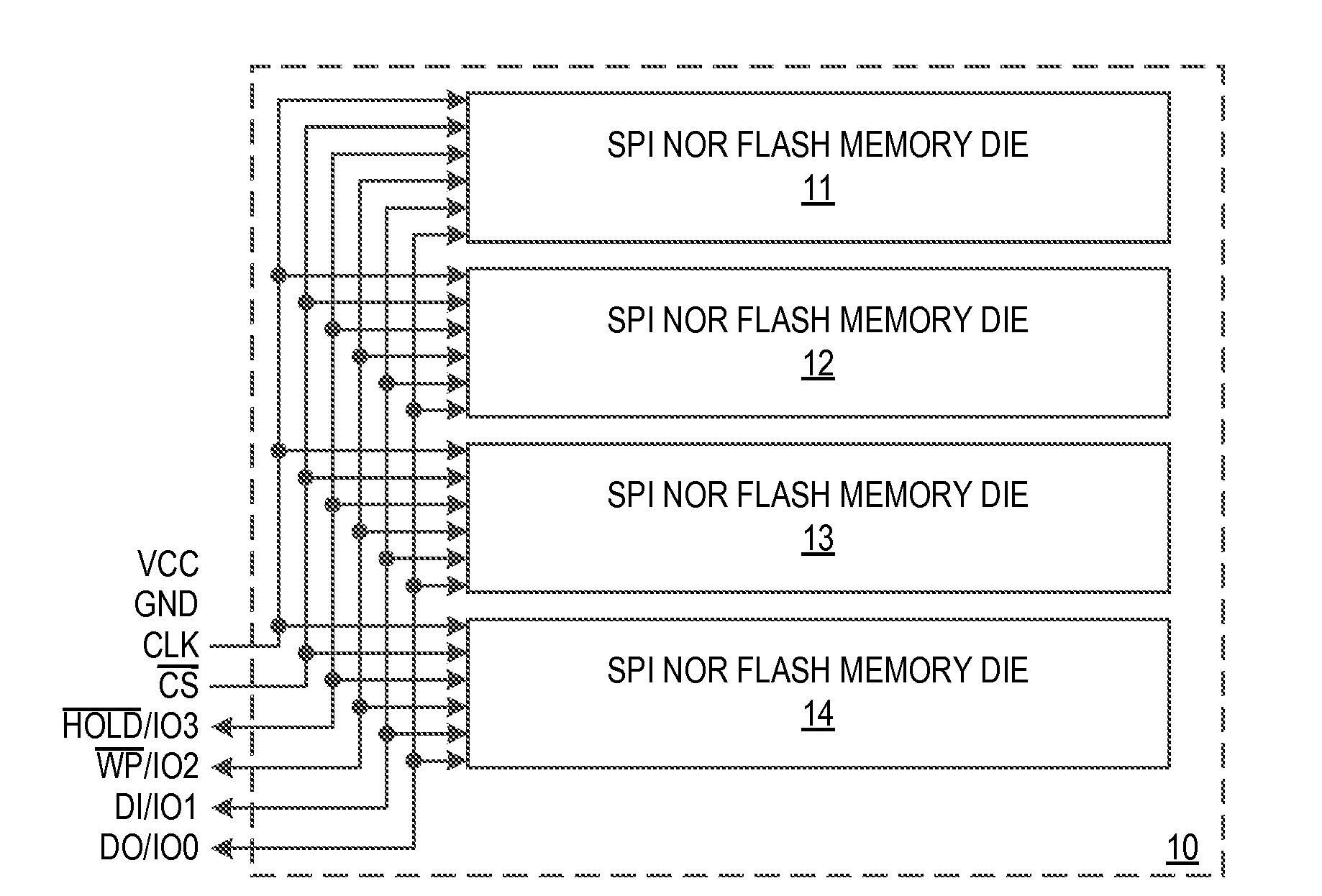
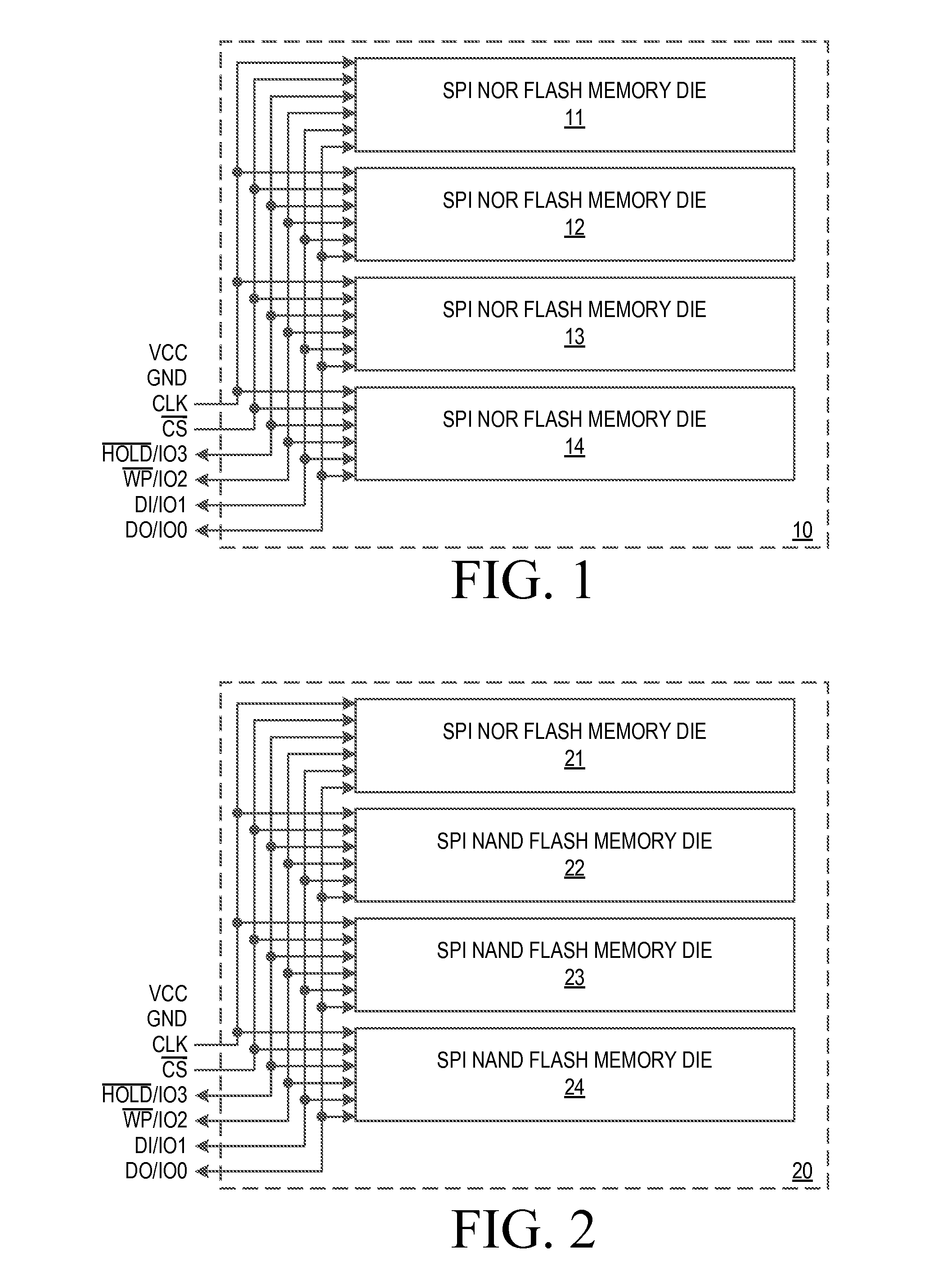
[0021]Any number of Serial Peripheral Interface (“SPI”) flash memory die may be stacked and packaged using any desired multi-chip packaging technique to realize any one or combination of various capabilities such as low per-bit cost, high density storage, code shadowing to RAM, and fast random access for “execute in place” applications, while preserving the advantages of the SPI interface. As used herein, the term “SPI flash memory die” refers to an integrated circuit die which includes a flash memory array of any type or types, and a set of interface pins which conform to the SPI protocol. During device manufacture, each of the stacked SPI flash memory die is assigned a unique identifier or “Die ID” relative to the other stacked SPI flash memory die in the package. During normal operations, the unique Die IDs are used by a Die Select instruction to enable one of the stacked SPI flash memory die to respond to subsequent instructions on the SPI interface, while disabling the other st...


PUM


Abstract

Any number of Serial Peripheral Interface (“SPI”) flash memory die may be stacked and packaged using any desired multi-chip packaging technique to realize any one or combination of various capabilities such as low per-bit cost, high density storage, code shadowing to RAM, and fast random access for “execute in place” applications, while preserving the advantages of the SPI interface. During device manufacture, each of the stacked die is assigned a unique identifier or “Die ID” relative to the other stacked die in the package. During normal operations, the unique Die IDs are used by a Die Select instruction to enable one of the stacked die to respond to subsequent instructions on the SPI interface, while disabling the other stacked die in the package from responding to subsequent instructions but for certain “Universal” instructions which include the Die Select instruction. Concurrent operations by the stacked die are supported.

Description

BACKGROUND OF THE INVENTION[0001]1. Field of the Invention[0002]The present invention relates to flash memory, and more particularly to flash memory devices which use stacked memory die and the Serial Peripheral Interface (“SPI”).[0003]2. Description of Related Art[0004]Serial flash memory has become a popular alternative to conventional parallel flash memory. Serial flash memory provides many advantages, including small footprint packaging, low pin-count, simplified printed circuit board layout, low power consumption, performance comparable to parallel flash memory, and reduced device and system -level costs. The Serial Peripheral Interface (“SPI”) is widely used in serial flash memory, and devices which are configurable for single-bit SPI or multi-bit SPI, including multi-bit instruction and / or address input and multi-bit data output, have become particularly popular. The SPI interface has many advantages. Single-bit SPI allows for broad compatibility, while multi-bit SPI when com...

Claims


Application Information

Patent Timeline
Patent Type & Authority Applications(United States)
IPC IPC(8): G11C5/06G11C16/10
CPCG11C16/107G11C5/063G11C5/02G11C5/04G11C16/08G11C16/16G11C16/20G11C16/32G11C2216/22G11C2216/24G11C2216/30H01L2924/181H01L2224/32145H01L2224/48247H01L2224/73265H01L2924/00012H01L2924/00
Inventor CHEN, HUISU, TENG
Owner WINBOND ELECTRONICS CORP
Why Eureka
Try Eureka