Storage cell, storage device, and magnetic head
a storage cell and magnetic head technology, applied in the field of storage cells, storage devices, magnetic heads, can solve problems such as lowering power consumption or increasing capacity, and achieve the effects of reducing power consumption of storage devices, enhancing reliability, and maintaining stably recorded information in storage cells
- Summary
- Abstract
- Description
- Claims
- Application Information
AI Technical Summary
Benefits of technology
Problems solved by technology
Method used
Image
Examples
experiment 1
[0171]The present experiment is an evaluation of perpendicular magnetic anisotropy of the storage cell 3 in FIG. 3, demonstrating effects in a case that carbon is inserted between the intermediate layer 16 and the storage layer 17. Sample structures for the experiment are as follows. As illustrated in FIG. 4,[0172]the base layer 14: a laminated film of a 10 nm-thick Ta film and a 10 nm-thick Ru film.[0173]the magnetization pinned layer 15: a laminated film of Co—Pt: 2 nm / Ru: 0.7 nm / [Co20Fe80]80B20: 1 nm.[0174]the storage layer 17: a 1.2 nm-thick [Co20Fe80]80B20 film.[0175]the cap layer 18: / a Ta: 5 nm film /
With the above-listed layers commonly provided, a structure of the intermediate layer 16 is as follows. Two samples were prepared.
[0176]As illustrated in A of FIG. 4 and B of FIG. 4,[0177]Sample 1 (A of FIG. 4) the intermediate layer 16: a 0.6 nm-thick MgO film, with no carbon inserted[0178]Sample 2 (B of FIG. 4) the intermediate layer 16: lamination of a 0.6 nm-thick MgO film and ...
experiment 2
[0190]The present experiment is an evaluation of TMR characteristics (the MR ratio) as to the structure of the storage cell 3 of the Experiment 1 by a CIPT (Current-In-Plane Tunneling) method. Sample structures are as follows, similarly to the Experiment 1.
[0191]As illustrated in FIG. 4, in each sample, layers in the lamination structure from the substrate to the cap layer are as follows.[0192]the base layer 14: a laminated film of 10 nm-thick Ta and 10 nm-thick Ru.[0193]the magnetization pinned layer 15: a laminated film of Co—Pt: 2 nm / Ru: 0.7 nm / [Co20Fe80]80B20: 1 nm.[0194]the storage layer 17: a 1.2 nm-thick [Co20Fe80]80B20 film.[0195]the cap layer 18: / a Ta: 5 nm film /
With the above-listed layers commonly provided, a structure of the intermediate layer 16 is as follows. Two samples were prepared.
[0196]As illustrated in A of FIG. 4 and C of FIG. 4,[0197]Sample 1 (A of FIG. 4) the intermediate layer 16: a 0.6 nm-thick MgO film, with no carbon inserted[0198]Sample 3 (C of FIG. 4) th...
experiment 3
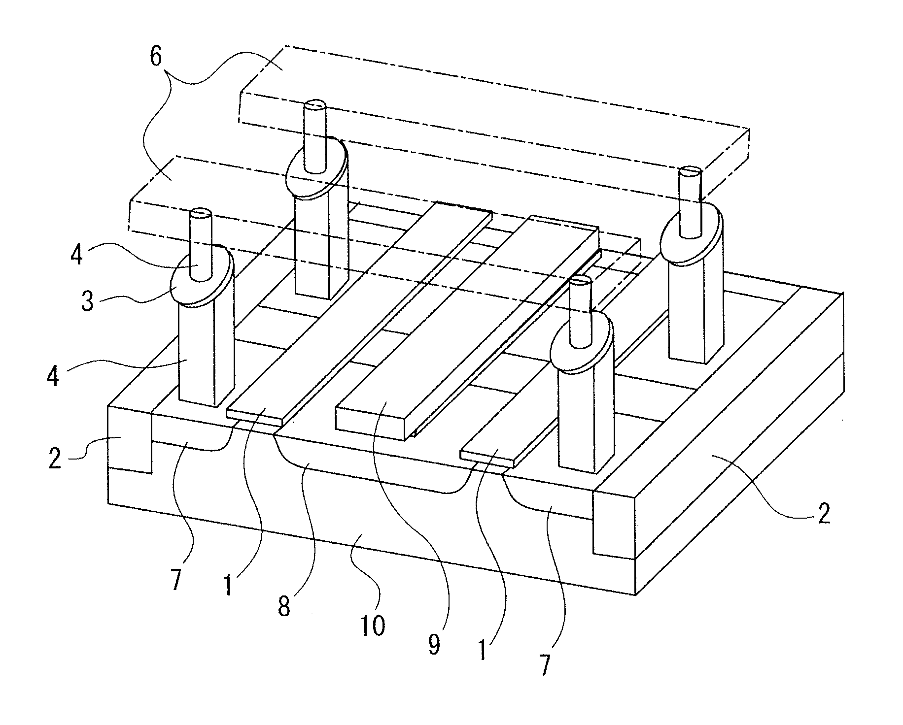
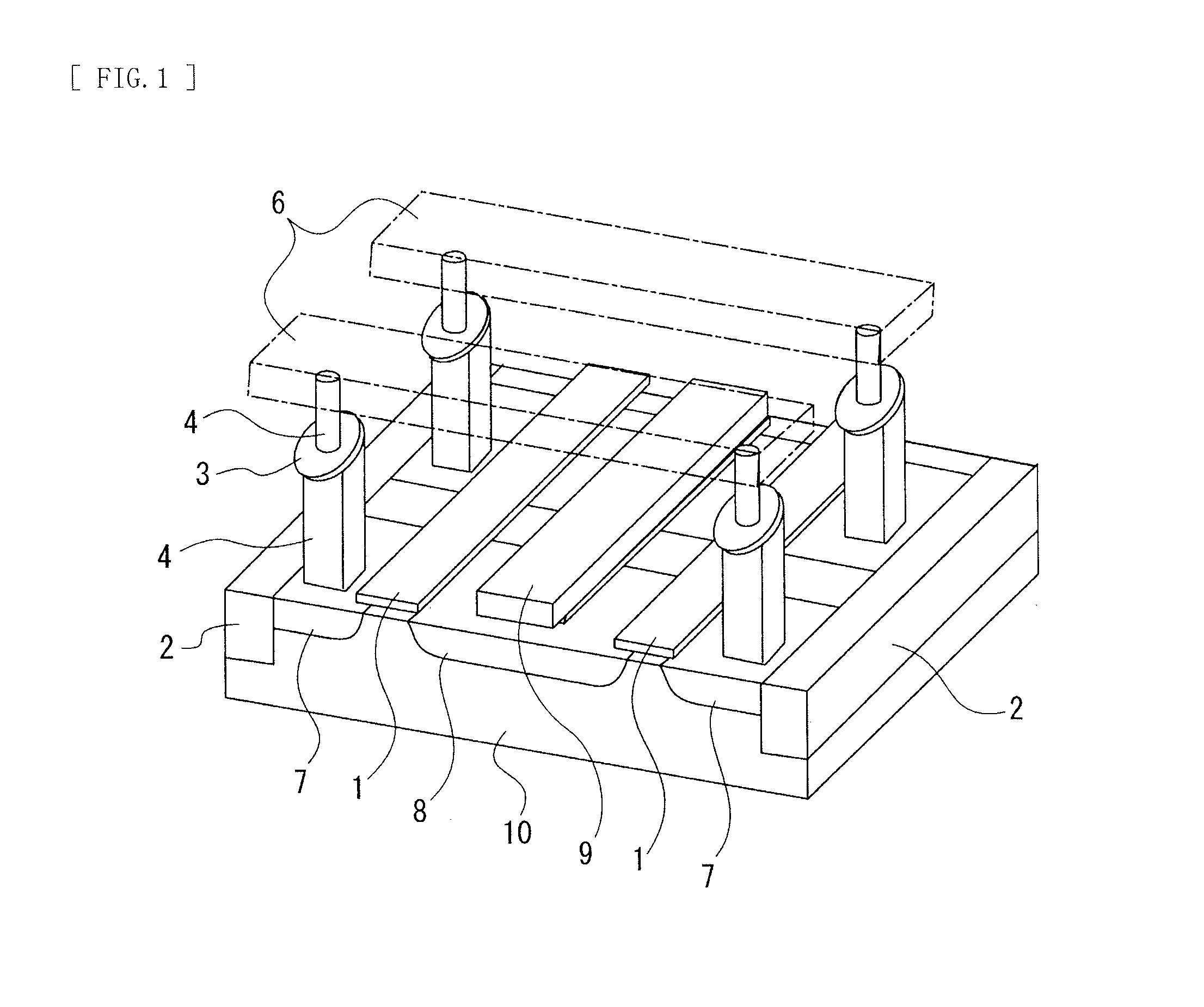
[0204]The present experiment is an evaluation of characteristics of a laminated structure in which carbon is inserted on both sides of the intermediate layer 16 and in the inside of the intermediate layer in the storage cell in FIG. 1. The minute cell was fabricated and subjected to measurement of a magnetic resistance curve.
[0205]In each sample, layers in the lamination structure from the substrate to the cap layer are as follows.
[0206]As illustrated in FIG. 4, layers in the lamination structure from the substrate to the cap layer are as follows.[0207]the base layer 14: a laminated film of 10 nm-thick Ta and 10 nm-thick Ru.[0208]the magnetization pinned layer 15: a laminated film of Co—Pt: 2 nm / Ru: 0.7 nm / [Co20Fe80]80B20: 1 nm.[0209]the storage layer 17: a 1.2 nm-thick [Co20Fe80]80B20 film.[0210]the cap layer 18: / a Ta: 5 nm film /
With the above-listed layers commonly provided, a structure of the intermediate layer 16 is as follows. Two samples were prepared.
[0211]As illustrated in A...
PUM
 Abstract
Description
Claims
Application Information


