Methods of manufacturing semiconductor devices

a manufacturing method and semiconductor technology, applied in the direction of vacuum evaporation coating, basic electric elements, coatings, etc., can solve the problem that the conductive layer may not be formed uniformly in the via hole, and achieve the effect of improving the horizontal deposition property and improving the vertical deposition property

Active Publication Date: 2015-09-10
SAMSUNG ELECTRONICS CO LTD
View PDF1 Cites 5 Cited by
  • Summary
  • Abstract
  • Description
  • Claims
  • Application Information

AI Technical Summary

Benefits of technology

[0036]According to an embodiment of the present inventive concepts, a layer deposition system may include a DC deposition chamber and an RF deposition chamber. Thus, a DC sputtering process having an improved horizontal deposition property and an RF sputtering process having an improved vertical deposition property may be combined so that a conductive layer having a uniform profile may be formed in a via hole. Therefore, the conductive layer may not be overhung at an upper portion of the via hole, and thus a void or a discontinuous formation of the conductive layer may be prevented.

Problems solved by technology

Thus, a desired deposition property, e.g., a gap-fill property may be deteriorated, and thus the conductive layer may not be formed uniformly in the via hole.

Method used


Image

  • Methods of manufacturing semiconductor devices
  • Methods of manufacturing semiconductor devices
  • Methods of manufacturing semiconductor devices

Examples


Embodiment Construction

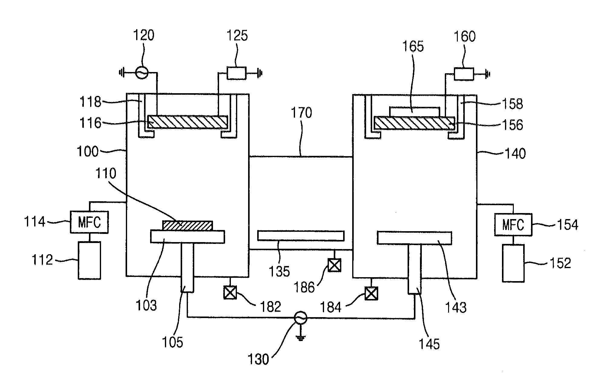
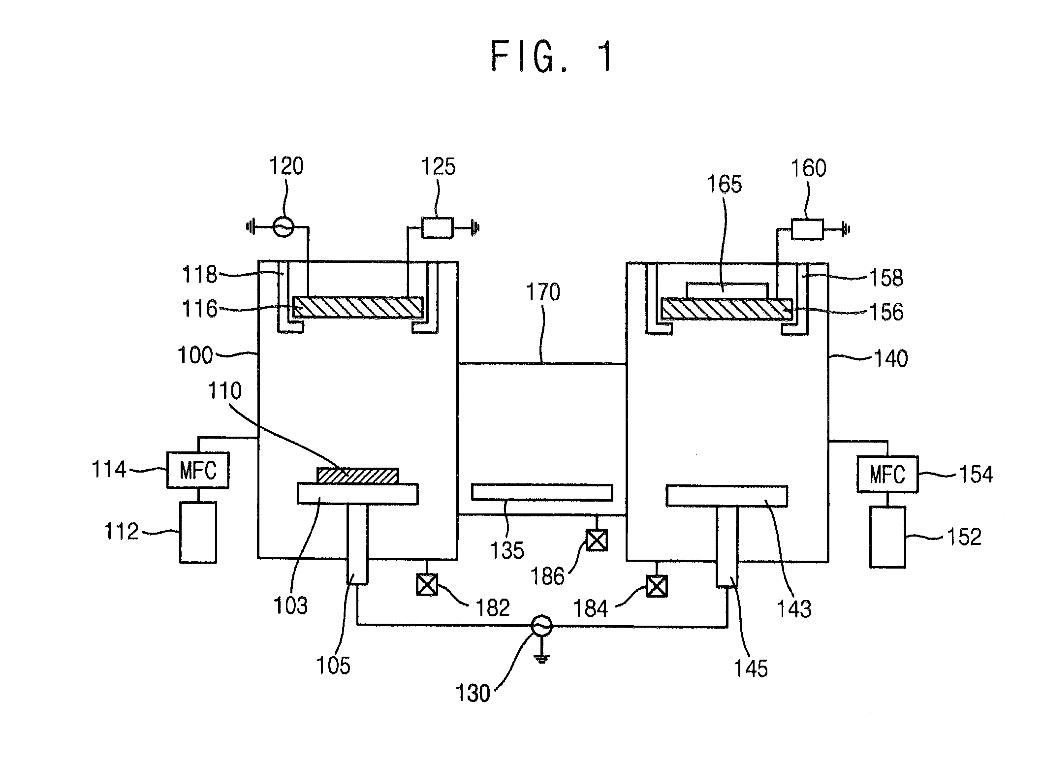
[0046]Various example embodiments will be described more fully hereinafter with reference to the accompanying drawings, in which some example embodiments are shown. The present inventive concepts may, however, be embodied in many different forms and should not be construed as limited to the example embodiments set forth herein. Rather, these example embodiments are provided so that this description will be thorough and complete, and will fully convey the scope of the present inventive concepts to those skilled in the art.

[0047]It will be understood that when an element or layer is referred to as being “on,”“connected to” or “coupled to” another element or layer, it can be directly on, connected or coupled to the other element or layer or intervening elements or layers may be present. Like numerals refer to like elements throughout. As used herein, the term “and / or” includes any and all combinations of one or more of the associated listed items.

[0048]It will be understood that, altho...


PUM

PropertyMeasurementUnit
DC poweraaaaaaaaaa
DC poweraaaaaaaaaa
frequencyaaaaaaaaaa

Abstract

In a method of manufacturing a semiconductor device, an insulating interlayer is formed on a substrate. The insulating interlayer is partially removed to form an opening. A barrier conductive layer is formed on a sidewall and a bottom of the opening. An RF sputtering process and a DC sputtering process are performed independently on the barrier conductive layer to form a seed layer. A plated layer is formed on the seed layer.

Description

CROSS-REFERENCE TO RELATED APPLICATION[0001]This application claims priority under 35 USC §119 to Korean Patent Application No. 10-2014-0026377, filed on Mar. 6, 2014 in the Korean Intellectual Property Office (KIPO), the contents of which are incorporated by reference herein in their entirety.BACKGROUND[0002]1. Technical Field[0003]Example embodiments relate to methods of manufacturing semiconductor devices. More particularly, example embodiments relate to methods of manufacturing semiconductor devices including conductive patterns.[0004]2. Description of the Related Art[0005]In a semiconductor device, a conductive pattern such as a via structure or a contact for an interconnection between wirings may be formed. For example, an insulation layer may be etched to form a via hole through which a lower wiring is exposed, and a conductive layer may be formed in the via hole.[0006]As a degree of integration becomes increased, a width of the via hole may be decreased. Thus, a desired depo...

Claims


Application Information

Patent Timeline
Patent Type & Authority Applications(United States)
IPC IPC(8): H01L21/768
CPCH01L21/76879H01L21/76832H01L21/76802H01L21/76831H01L21/2855H01L23/481H01L21/76807H01L21/76843H01L21/76873C23C14/185C23C14/3464H01L2924/0002H01L2924/00H01L21/76871
Inventor MOON, HYO-JEONGNOH, WOO-CHEOLJANG, WOO-JINKIM, HUNSHIN, HONG-JAE
Owner SAMSUNG ELECTRONICS CO LTD
Why Eureka
Try Eureka