Optimized ESD Clamp Circuitry

a clamp circuit and clamp technology, applied in the field of electronic circuits, can solve the problems that the circuitry of the semiconductor device (e.g., the integrated circuit, the ics) is particularly vulnerable to adverse effects, damage or destruction, and achieve the effect of saving the area and reducing the rc time constan

Active Publication Date: 2015-09-24
APPLE INC
View PDF6 Cites 20 Cited by
  • Summary
  • Abstract
  • Description
  • Claims
  • Application Information

AI Technical Summary

Benefits of technology

[0009]In some embodiments, each clamping transistor may be associated with a dedicated sensor circuit. In other embodiments, at least some of the sensor circuits may be configured to activate two or more clamping circuits, which may realize some area savings. Furthermore, a greater quantity of CDM sensors may be implemented than HBM sensors. This may save area relative to an IC in

Problems solved by technology

Semiconductor devices (e.g., integrated circuits, or ICs) may be particularly vulnerable to the adv

Method used


Image

  • Optimized ESD Clamp Circuitry
  • Optimized ESD Clamp Circuitry
  • Optimized ESD Clamp Circuitry

Examples


Embodiment Construction

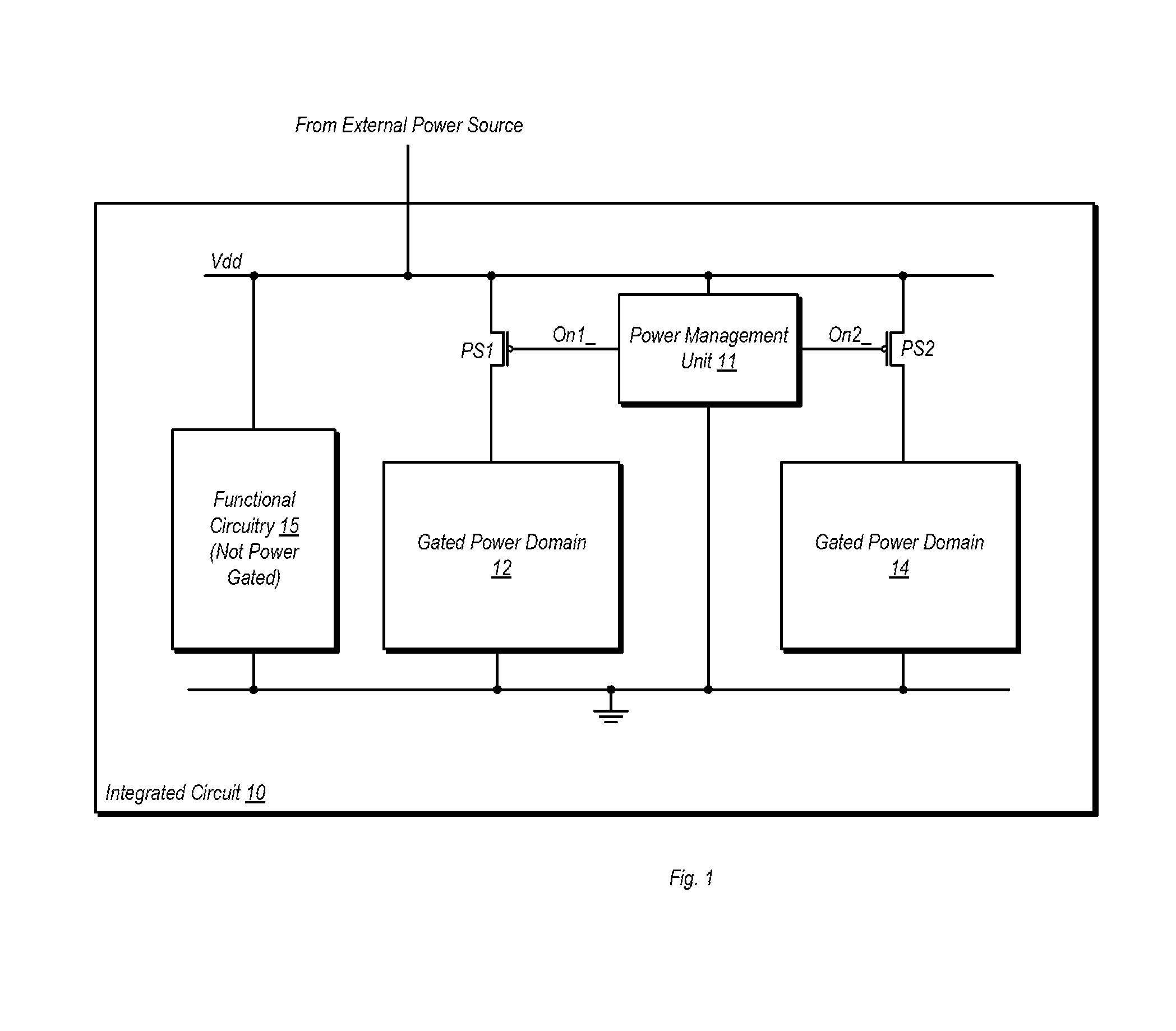
[0023]FIG. 1 is a block diagram of one embodiment of an IC having multiple power domains. In the embodiment shown, IC 10 includes a global power domain (powered from voltage node Vdd) and two gated power domains 12 and 14. Functional circuitry 15 in the embodiment shown is within the global power domain, and receives power any time voltage node Vdd is receiving power from an external power source. The functional circuitry 15 may perform some of the useful work performed by IC 10. As defined herein, a global power domain may be circuitry that receives power at any time it is being supplied to IC 10 from an external source (which may include receiving power via an on-chip voltage regulator). Furthermore, a global voltage node may be defined as a voltage node that receives (and distributes) power at a specified supply voltage from whenever power is being supplied from the external source.

[0024]A gated power domain may be defined as a power domain in which power is received from the glo...


PUM


Abstract

ESD protection circuitry is disclosed. In one embodiment, an integrated circuit includes first and second sensor circuits. The first sensor circuit has a first resistive-capacitive (RC) time constant, while the second sensor circuit has a second RC time constant. The RC time constant of the first sensor circuit is at least one order of magnitude greater than that of the second sensor circuit. A first clamp transistor is coupled to and configured to be activated by the first sensor circuit responsive to the latter detecting an ESD event. A second clamp transistor is coupled to and configured to be activated by the second sensor circuit responsive to the latter detecting the ESD event.

Description

BACKGROUND[0001]1. Technical Field[0002]This disclosure relates to electronic circuits, and more particularly, to circuits arranged to prevent damage resulting from electro-static discharge.[0003]2. Description of the Related Art[0004]Electro-static discharge (ESD) is a sudden electrical current flow between two charged surfaces. Often times, a significant difference in voltage potential may exist between the two charged surfaces. When the surfaces are electrically shorted together, come into contact, or dielectric breakdown occurs therebetween, the surfaces may discharge until the difference in voltage is effectively zero. Since the voltage difference prior to discharge may be large, the corresponding currents during discharge may also be large.[0005]Semiconductor devices (e.g., integrated circuits, or ICs) may be particularly vulnerable to the adverse effects of ESD. The large currents that can be produced by ESD can damage or destroy circuitry. Accordingly, during manufacturing a...

Claims


Application Information

Patent Timeline
IPC IPC(8): H01L27/02H02H9/04
CPCH02H9/046H01L27/0285H02H3/20H02H3/22
Inventor DABRAL, SANJAYFAN, XIAOFENGJOORDENS, GEERTJAN
Owner APPLE INC
Why Eureka
Try Eureka