MEMS package structure and manufacturing method thereof

Active Publication Date: 2015-10-08
HIMAX DISPLAY INC
View PDF1 Cites 2 Cited by
  • Summary
  • Abstract
  • Description
  • Claims
  • Application Information

AI Technical Summary

Benefits of technology

[0025]Based on the above-mentioned description, the MEMS package structure of the present invention applies the first cover covering the MEMS device to prevent the MEMS device from pollution and to provide a first moisture protection for the MEMS device. In addition, the MEMS device and the first cover are disposed in the recess of the base, the second cover is sealed to the base through the glass fit or the first metal frame around the second cover is sealed to the base through the first sealing medium, so that the combination of the second cover, the base and the glass frit or the combination of the second cover, the base, the first metal frame and the first sealing medium provide the se

Problems solved by technology

However, in the macroscopic world of the entire package structure, the MEMS device is extremely fragile and may be impacted by slight static electricity or surface tension at any moment to cause failure.
However, glue may crack and occur the outgassing phenomena easily in th

Method used


Image

  • MEMS package structure and manufacturing method thereof
  • MEMS package structure and manufacturing method thereof
  • MEMS package structure and manufacturing method thereof

Examples


Embodiment Construction

[0031]Reference will now be made in detail to the present preferred embodiments of the invention, examples of which are illustrated in the accompanying drawings. Wherever possible, the same reference numbers are used in the drawings and the description to refer to the same or like parts.

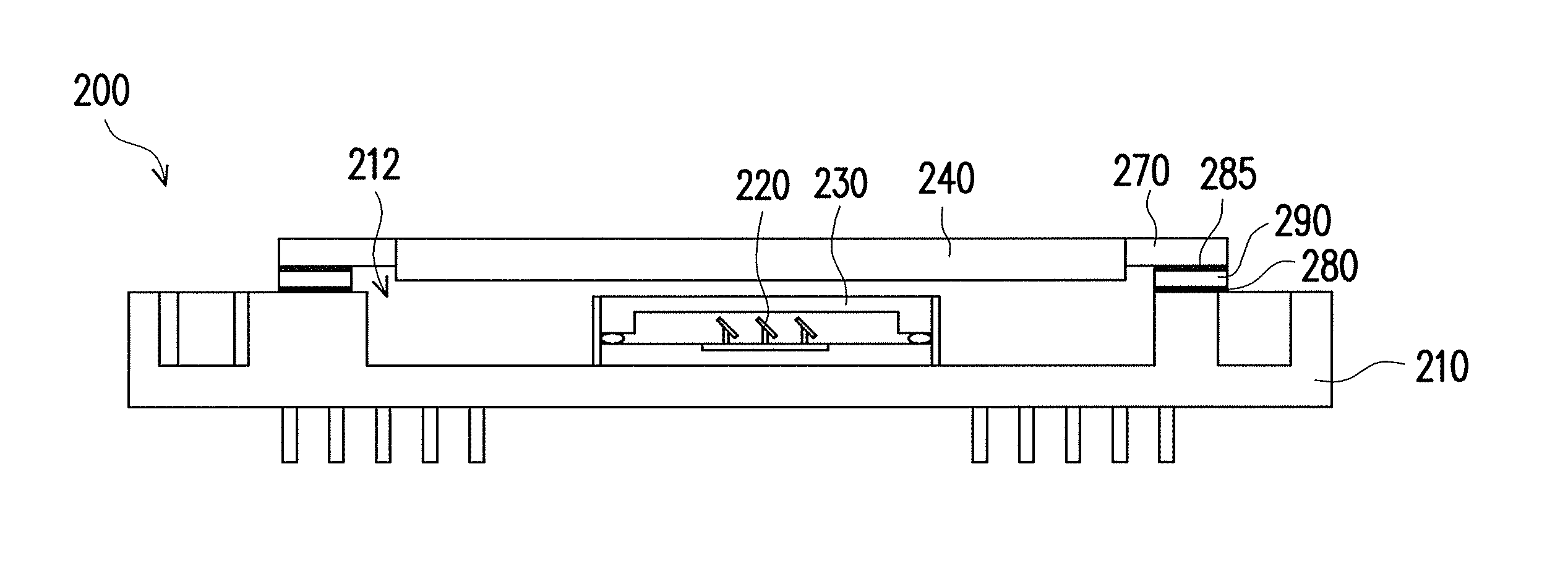
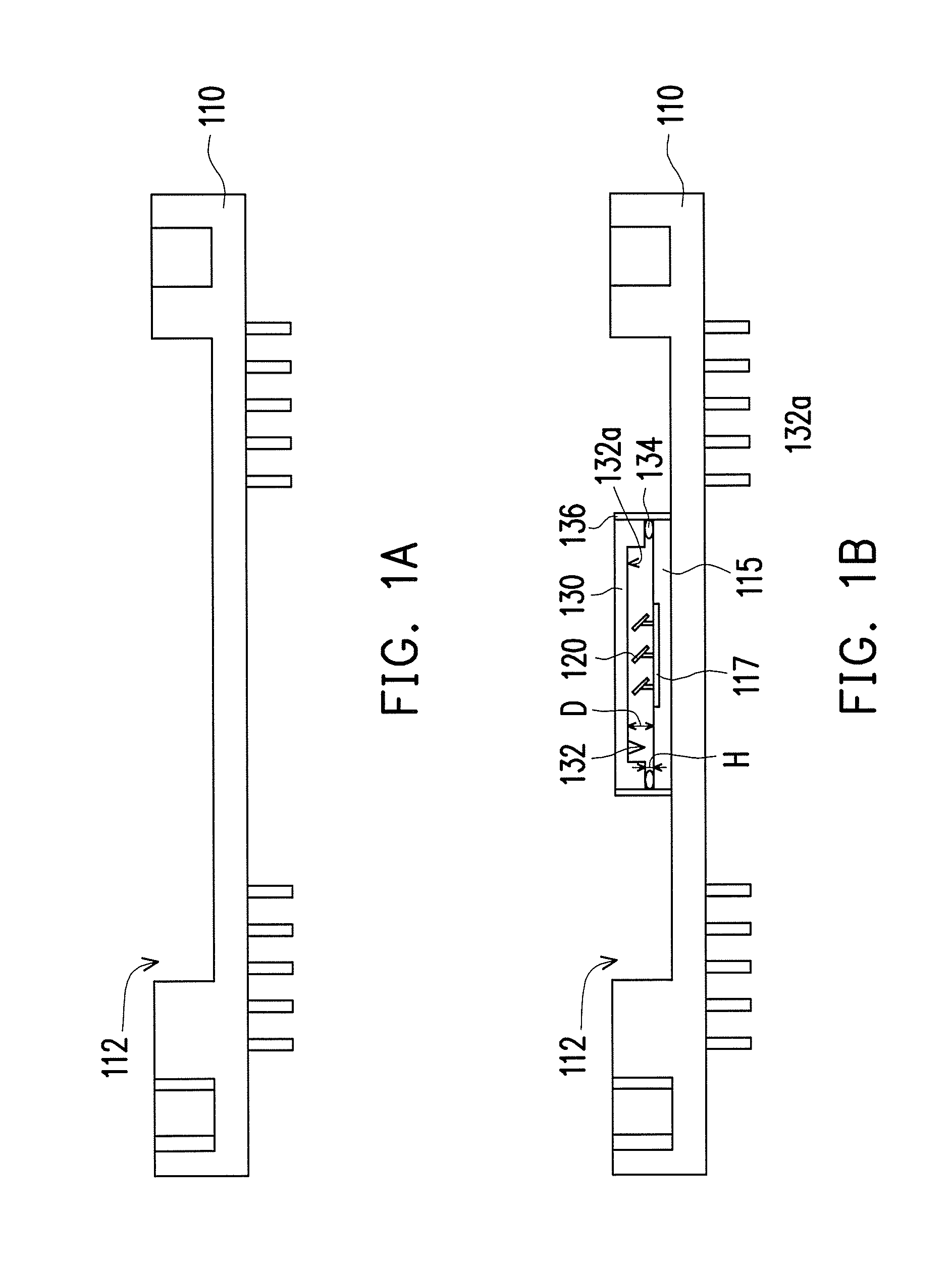
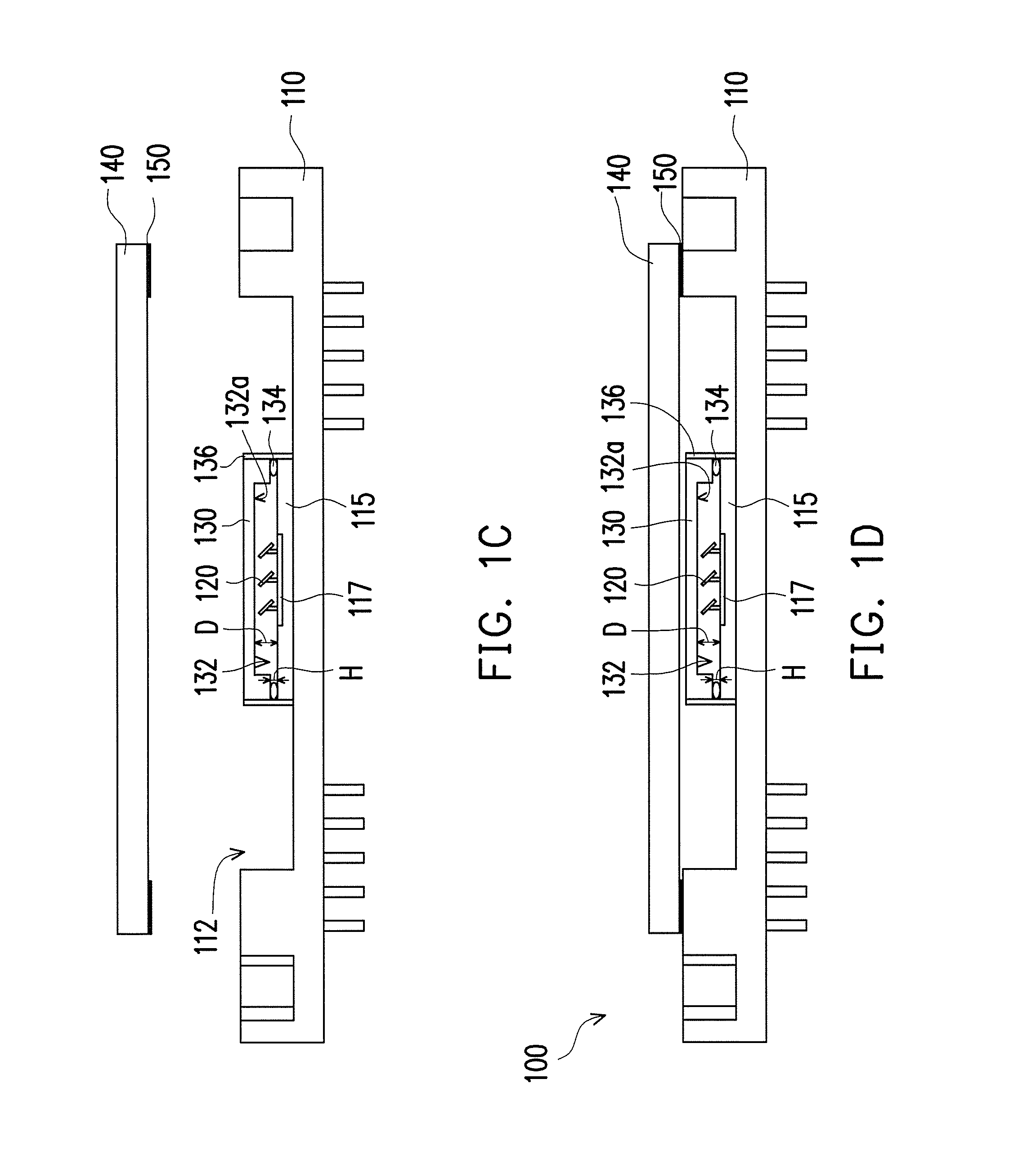
[0032]FIG. 1A to FIG. 1D are schematic views of a manufacturing method of a MEMS package structure according to an embodiment of the invention. A manufacturing method of a microelectromechanical system (MEMS) package structure comprises the following steps. Referring to FIG. 1A, provide a base 110, wherein the base 110 comprises a recess 112. In the embodiment, material of the base 110 is ceramic, but material of the base 110 is not limited thereto.

[0033]Then, referring to FIG. 1B, dispose at least one MEMS device 120 covered by a first cover 130 in the recess 112 of the base 120. The first cover 130 covering on the MEMS devices 120 is capable of preventing the MEMS devices 120 from pollution (such a...


PUM

PropertyMeasurementUnit
Temperatureaaaaaaaaaa
Melting pointaaaaaaaaaa
Thermal expansion coefficientaaaaaaaaaa

Abstract

A MEMS package structure includes a base, a MEMS device, a first cover, a second cover and a glass frit. The base includes a recess. The MEMS device is disposed in the recess. The first cover is disposed in the recess and covering the MEMS device. The second cover is disposed on the base and covering the recess. The glass frit is disposed between the base and the second cover. A MEMS package structure includes the base, the MEMS device, the first cover, a second cover, a first metal frame and a first sealing medium. The first metal frame is disposed around the second cover, and the second cover and the first metal frame collectively are disposed on the base and covering the recess. The first sealing medium is disposed between the first metal frame and the base. Manufacturing methods of the MEMS package structures above are further provided.

Description

CROSS-REFERENCE TO RELATED APPLICATION[0001]This application is a continuation-in-part application of and claims the priority benefit of U.S. application Ser. No. 14 / 167,819, filed on Jan. 29, 2014, now allowed. The entirety of the above-mentioned patent application is hereby incorporated by reference herein and made a part of this specification.BACKGROUND OF THE INVENTION[0002]1. Field of the Invention[0003]The present invention generally relates to a package structure and a manufacturing method thereof. More particularly, the present invention relates to a microelectromechanical system (MEMS) package structure and a manufacturing method thereof.[0004]2. Description of Related Art[0005]Microelectromechanical system (MEMS) is a microelectromechanical device fabricated in a microminiaturized package structure, and the fabricating technique thereof is quite similar to the technique of fabricating integrated circuits (ICs). However, interactions, for example, about mechanics, optics, o...

Claims


Application Information

Patent Timeline
IPC IPC(8): B81B7/00B81C1/00
CPCB81B7/0058B81B2201/042B81C1/00269B81B7/0041B81C2203/019G02B26/0833G02B27/0006H01L2924/16195H01L2924/16235
Inventor WU, TUNG-FENGCHEN, WEI-HSIAOSU, CHUN-HAOCHEN, JUI-WENCHENG, MAO-CHIEN
Owner HIMAX DISPLAY INC
Why Eureka
Try Eureka