
Semiconductor Device, and Module and Electronic Appliance Including the Same

Active Publication Date: 2015-10-08
SEMICON ENERGY LAB CO LTD
View PDF1 Cites 9 Cited by
  • Summary
  • Abstract
  • Description
  • Claims
  • Application Information

AI Technical Summary

Benefits of technology

The present invention aims to provide a novel semiconductor device and its driving method, as well as a novel manufacturing method. The semiconductor device can display images with improved quality, have high resolution, reduced variation in luminance between pixels, and / or have a smaller number of terminals. This will result in better overall performance and usability of the semiconductor device.

Problems solved by technology

The variation in the threshold voltage of the driving transistor between a plurality of pixels is one cause of a reduction in the display quality of the display device.
It is highly difficult to make the threshold voltages of driving transistors in such a large number of pixels completely equal to each other.

Method used


Image

  • Semiconductor Device, and Module and Electronic Appliance Including the Same
  • Semiconductor Device, and Module and Electronic Appliance Including the Same
  • Semiconductor Device, and Module and Electronic Appliance Including the Same

Examples


embodiment 1

[0071]In this embodiment, a light-emitting device including a light-emitting element is described as an example of a semiconductor device. The light-emitting device of this embodiment can function as a display device.

>

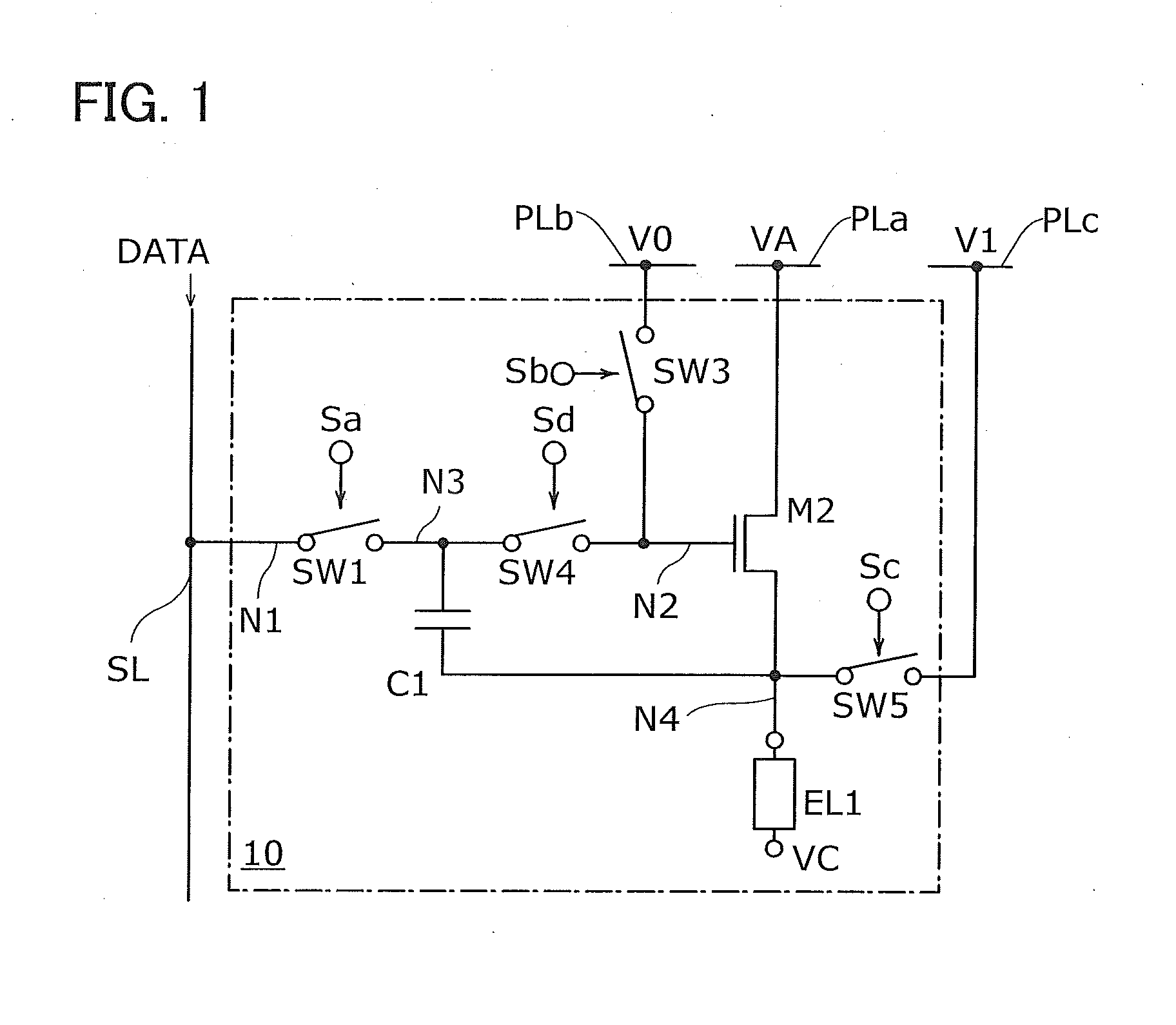
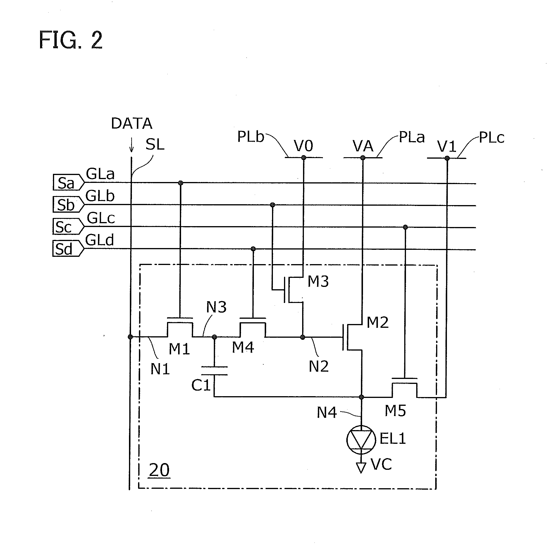
[0072]FIG. 1 illustrates an example of a configuration of a pixel of the light-emitting device. As illustrated in FIG. 1, a pixel 10 includes a switch SW1, a switch SW3, a switch SW4, a switch SW5, a transistor M2, a capacitor C1, and a light-emitting element EL1. The pixel 10 is electrically connected to a wiring SL, a wiring PLa, a wiring PLb, and a wiring PLc. A pixel portion of the light-emitting device is provided with a plurality of pixels 10 arranged in array.

[0073]The conduction state of SW1 is controlled by a signal Sa. The conduction state of SW3 is controlled by a signal Sb. The conduction state of SW4 is controlled by a signal Sd. The conduction state of the switch SW5 is controlled by a signal Sc. In the example of FIG. 1, the conduction states of the four...

embodiment 2

[0100]In this embodiment, an active matrix display device is described as an example of a semiconductor device. Specifically, a configuration example, a driving method example, and the like of an active matrix display device including the pixels 10 in the pixel portion are described.

>

[0101]FIG. 7 is a block diagram illustrating an example of the configuration of a display device.

[0102]As illustrated in FIG. 7, a display device 50 includes a controller 51, a power management unit (PMU) 52, a power supply circuit 53, a pixel portion 60, a gate driver circuit 61, a source driver circuit 62, and the like. Here, the gate driver circuit 61 and the source driver circuit 62 may be collectively referred to as a peripheral circuit 63.

[0103]The pixel portion 60 includes a plurality of pixels 65 arranged in array, a plurality of wirings 66 arranged in the vertical direction, and a plurality of wirings 67 arranged in the horizontal direction. The pixels 65 in the same row are connected to the wi...

embodiment 3

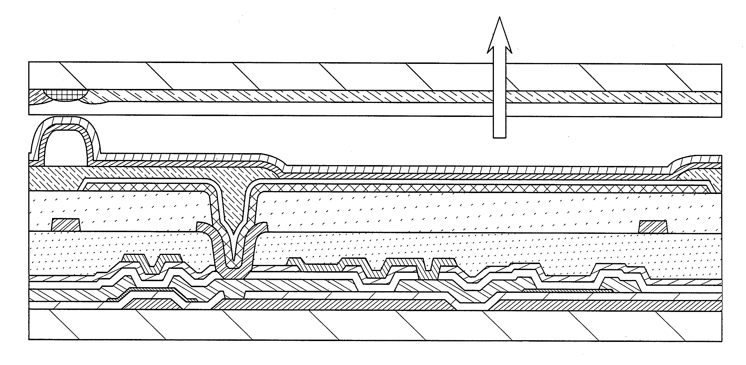
[0169]In this embodiment, an active matrix display device is described as an example of a semiconductor device. As an example, a device structure of the display panel of Embodiment 2 and a manufacturing method thereof are described. More specifically, a structure example of the display panel 100 (FIG. 10) using the element substrate 101, a manufacturing method example thereof, and the like are described.

(Device Structure and the Like of Semiconductor Element)

[0170]There is no particular limitation on a device structure of a semiconductor element such as a transistor included in the element substrate 101. A transistor suitable for characteristics of a circuit formed in the element substrate 101 may be selected. As the device structure of the transistor, for example, a top-gate type, a bottom-gate type, a dual-gate type provided with both a gate (front gate) and a bottom gate, and a multi-gate type including a plurality of gate electrodes for one semiconductor layer can be given. In a...


PUM


Abstract

First to fourth switches are provided so that conduction states are able to be controlled independently of each other. The first switch, the third switch, and the second switch are electrically connected in series between a first wiring and a third wiring. The fourth switch has a function of controlling a conduction state between the light-emitting element and a fourth wiring. In a first transistor, a gate is electrically connected to a node to which the third switch and the second switch are electrically connected, one of a source and a drain is electrically connected to a second wiring, and the other is electrically connected to the light-emitting element. A capacitor includes first and second electrodes, the first electrode is electrically connected to a node to which the first switch and the third switch are electrically connected, and the second electrode is electrically connected to the light-emitting element.

Description

BACKGROUND OF THE INVENTION[0001]1. Field of the Invention[0002]One embodiment of the present invention relates to a semiconductor device, a driving method thereof, a manufacturing method thereof, and the like.[0003]Note that one embodiment of the present invention is not limited to the above technical field. The technical field of one embodiment of the invention disclosed in this specification and the like relates to an object, a method, or a manufacturing method. In addition, one embodiment of the present invention relates to a process, a machine, manufacture, or a composition (a composition of matter). Therefore, more specifically, as the technical field of one embodiment of the present invention disclosed in this specification, a semiconductor device, a display device, a liquid crystal display device, a light-emitting device, a lighting device, a power storage device, a storage device, a driving method of them, or a manufacturing method of them can be given.[0004]2. Description ...

Claims


Application Information

Patent Timeline
IPC IPC(8): H01L27/12
CPCH01L27/124H01L27/1255H01L29/78648H01L27/1225H01L27/1251G09G3/3233G09G3/3266G09G3/3291G09G2300/0819G09G2300/0842G09G2300/0861G09G2310/0248G09G2310/0286G09G2310/0297H01L33/382H01L33/62
Inventor MIYAKE, HIROYUKI
Owner SEMICON ENERGY LAB CO LTD
Learn More