Package material for packaging photoelectric device and package

a photoelectric device and packaging technology, applied in the direction of basic electric elements, semiconductor devices, electrical equipment, etc., can solve the problems of uniform light at a large viewing angle, inability to produce uniform light in packages, and inability to refractive and scatter light well, etc., to achieve the lowest correlated color temperature of packages, reduce the quantity of phosphor particles used in packages, and improve the quantity of light output

Inactive Publication Date: 2015-10-08
GENESIS PHOTONICS
View PDF0 Cites 7 Cited by
  • Summary
  • Abstract
  • Description
  • Claims
  • Application Information

AI Technical Summary

Benefits of technology

[0010]As the above mentioned, the disclosure disposes the first molding portion, which is doped with the nano-scale metal oxide particles, and the second molding portion, which is doped with the submicron-scale metal oxide particles, on the photoelectric device, such that the whole refractive index of the first molding portion is larger than the whole refractive index of the second molding portion, wherein the first molding portion is close to the photoelectric device and the second molding portion is away from the photoelectric device. Accordingly, light emitted by the light emitting diode will pass through the first molding portion with larger refractive index first, so as to enhance the quantity of light output. Afterward, the light will pass through the second molding portion and be scattered by the submicron-scale metal oxide particles, so as to generate uniform light. Furthermore, when the phosphor particles are doped in the second molding portion or the phosphor portion is disposed on the second molding portion, the difference between the highest correlated color temperature and the lowest correlated color temperature of the package of the disclosure will decrease. Accordingly, the light emitted by the package will be more uniform and the quantity of phosphor particles used in the package can be reduced.

Problems solved by technology

In general, if there are only phosphor particles doped in the molding compound 14, light cannot be refracted and scattered well, such that the LED package 1 cannot generate uniform light.
Especially, the light at large viewing angle will be more non-uniform, such that the visual effect will be influenced.

Method used


Image

  • Package material for packaging photoelectric device and package
  • Package material for packaging photoelectric device and package
  • Package material for packaging photoelectric device and package

Examples


first embodiment

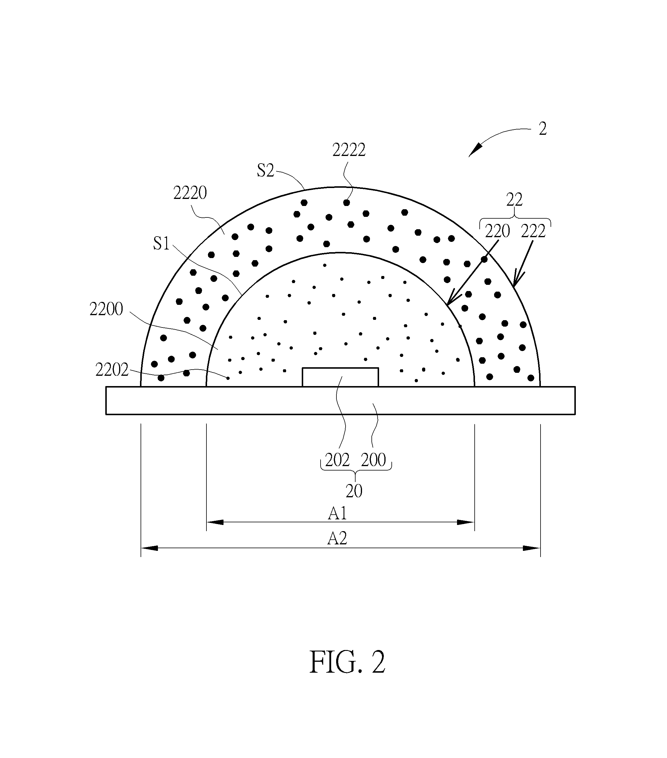
[0020]Referring to FIG. 2, FIG. 2 is a schematic view illustrating a package 2 according to the disclosure. As shown in FIG. 2, the package 2 comprises a photoelectric device 20 and a package material 22, wherein the package material 22 is used for packaging the photoelectric device 20. The photoelectric device 20 comprises a support 200 and a light emitting diode (LED) 202, wherein the LED 202 is disposed on the support 200. The package material 22 is disposed on the support 200 and covers the LED 202. The package material 22 comprises a first molding portion 220 and a second molding portion 222.

[0021]The first molding portion 220 is disposed on the support 200 of the photoelectric device 20 and covers the LED 202. The first molding portion 220 comprises a first molding compound 2200 and a plurality of nano-scale metal oxide particles 2202, wherein the nano-scale metal oxide particles 2202 are doped in the first molding compound 2200. In an embodiment, the nano-scale metal oxide pa...

second embodiment

[0024]Referring to FIG. 3 along with FIG. 2, FIG. 3 is a schematic view illustrating a package 3 according to the disclosure. The main difference between the package 3 and the aforementioned package 2 is that the package material 22 of the package 3 further comprises a plurality of phosphor particles 224 doped in the second molding compound 2220, wherein a concentration of the phosphor particles 224 in the second molding compound 2220 is between 3 wt % and 40 wt %. It should be noted that the concentration of the phosphor particles 224 maybe lower if the package 3 has a reflective layer or the like, and the concentration of the phosphor particles 224 may be higher if the package 3 does not has a reflective layer or the like. In this embodiment, the light scattered by the submicron-scale metal oxide particles 2222 may excite more phosphor particles 224, so as to reduce the quantity of phosphor particles 224 used in the package 3. Furthermore, since the submicron-scale metal oxide par...

third embodiment

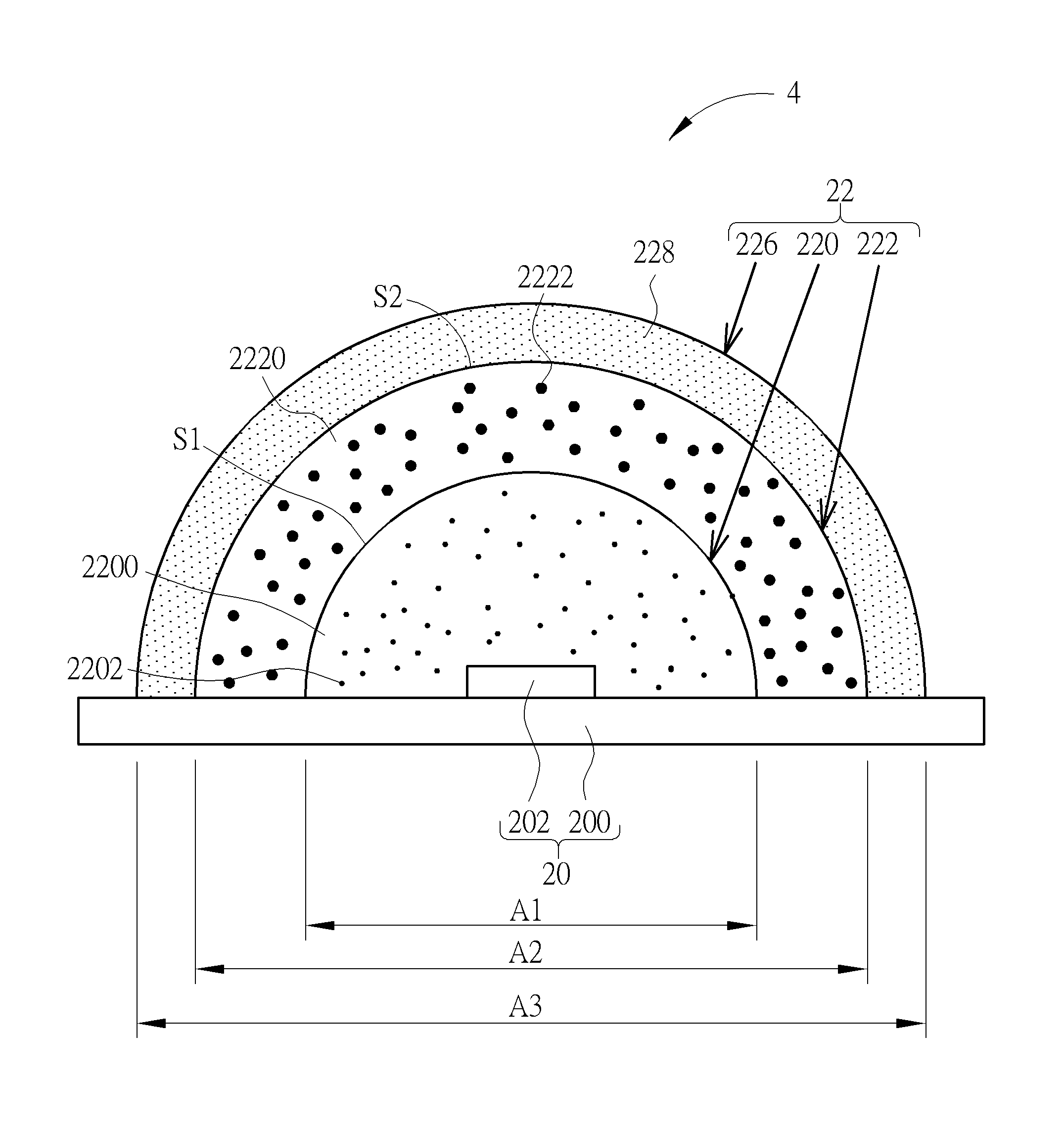
[0025]Referring to FIG. 4 along with FIG. 2, FIG. 4 is a schematic view illustrating a package 4 according to the disclosure. The main difference between the package 4 and the aforementioned package 2 is that the package material 22 of the package 4 further comprises a phosphor portion 226 disposed on the second molding compound 222, wherein the phosphor portion 226 comprises a plurality of phosphor particles 228. In this embodiment, the phosphor portion 226 covers the second molding portion 222, such that a projection area A3 of the phosphor portion 226 projected on the support 200 is larger than the projection area A2 of the second molding portion 222 projected on the support 200. Accordingly, the light scattered by the submicron-scale metal oxide particles 2222 can be used to excite the phosphor particles 228 effectively. However, the projection area A3 of the phosphor portion 226 projected on the support 200 may be equal to the projection area A2 of the second molding portion 22...


PUM

PropertyMeasurementUnit
roughnessaaaaaaaaaa
primary diameteraaaaaaaaaa

Abstract

A package material for packaging a photoelectric device includes a first molding portion and a second molding portion. The first molding portion is disposed on the photoelectric device. The first molding portion includes a first molding compound and a plurality of nano-scale metal oxide particles, wherein the nano-scale metal oxide particles are doped in the first molding compound. The second molding portion is disposed on the first molding portion and away from the photoelectric device. The second molding portion includes a second molding compound and a plurality of submicron-scale metal oxide particles, wherein the submicron-scale metal oxide particles are doped in the second molding compound. A whole refractive index of the first molding portion is larger than a whole refractive index of the second molding portion.

Description

BACKGROUND OF THE INVENTION[0001]1. Field of the Invention[0002]The invention relates to a package material and a package and, more particularly, to a package material for packaging a photoelectric device and a package.[0003]2. Description of the Prior Art[0004]Referring to FIG. 1, FIG. 1 is a schematic view illustrating a light emitting diode (LED) package 1 of the prior art. The LED package 1 includes a package substrate 10, a light emitting diode chip 12 and a molding compound 14. The light emitting diode chip 12 is disposed on the package substrate 10 and the molding compound 14 is dispensed on the package substrate 10 and the light emitting diode chip 12, so as to package the light emitting diode chip 12. In general, if there are only phosphor particles doped in the molding compound 14, light cannot be refracted and scattered well, such that the LED package 1 cannot generate uniform light. Especially, the light at large viewing angle will be more non-uniform, such that the visu...

Claims


Application Information

Patent Timeline
Patent Type & Authority Applications(United States)
IPC IPC(8): H01L33/58H01L33/50H01L33/54H01L33/56
CPCH01L33/58H01L33/56H01L2933/0091H01L33/54H01L33/502H01L33/507
Inventor HUANG, KUAN-CHIEHTSENG, CHUN-MINGLU, WEN-JIEWU, TSUNG-TSESU, WEI-LINGLIAO, KUAN-YUNGSHEU, GWO-JIUN
Owner GENESIS PHOTONICS
Why Eureka
Try Eureka