System and Method for Signal Generation

a signal generation and system technology, applied in the field of terahertz signal generation, can solve the problems of limited terahertz power generation of prior cmos, low relevant frequency range, and high relevance of electronics

Inactive Publication Date: 2015-10-08
CORNELL UNIVERSITY
View PDF1 Cites 10 Cited by
  • Summary
  • Abstract
  • Description
  • Claims
  • Application Information

AI Technical Summary

Benefits of technology

[0055]FIG. 37 is a table showing a performance compari

Problems solved by technology

Unfortunately, the bandwidth of the prior CMOS works is limited.
Unfortunately, it is well known that a “terahertz gap” exists, which keeps the generated terahertz power low.
This is because the relevant frequency range is too high for electronics, and too low for optics.
First, despite the aggressive trend to scale down CMOS, the maximum frequency of oscillation, fmax, of a CMOS transistor is still below 300 GHz, especially when device interconnects are included.
This sets a theoretical limitation, beyond which no fundamental oscillation nor power amplification is possible.
Second, the thinner gate oxide in the advanced technology node results in lower breakdown voltage.
This severely reduces the output power of the device, which is strongly correlated to the voltage swing.
Third, the passive met

Method used


Image

  • System and Method for Signal Generation
  • System and Method for Signal Generation
  • System and Method for Signal Generation

Examples


Embodiment Construction

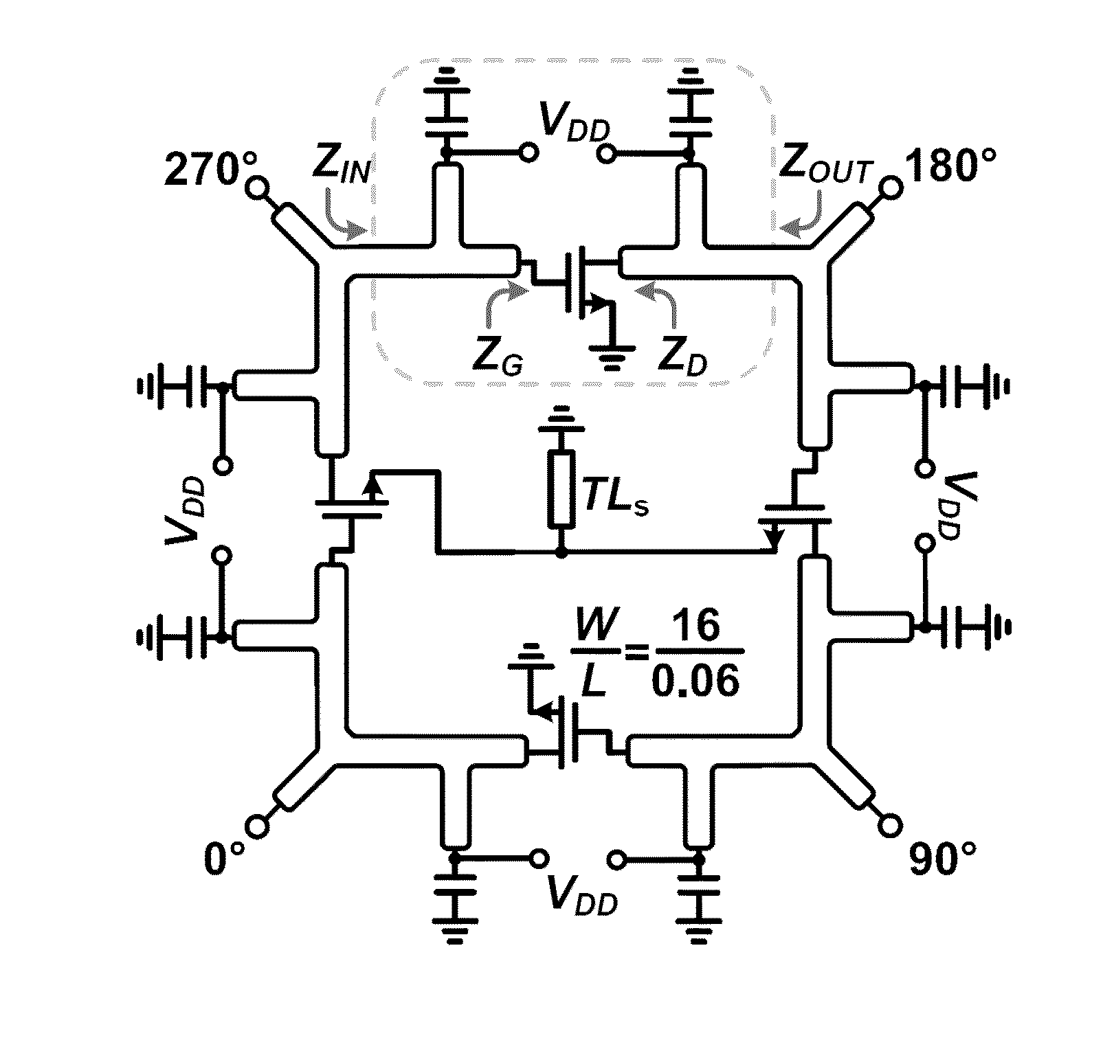
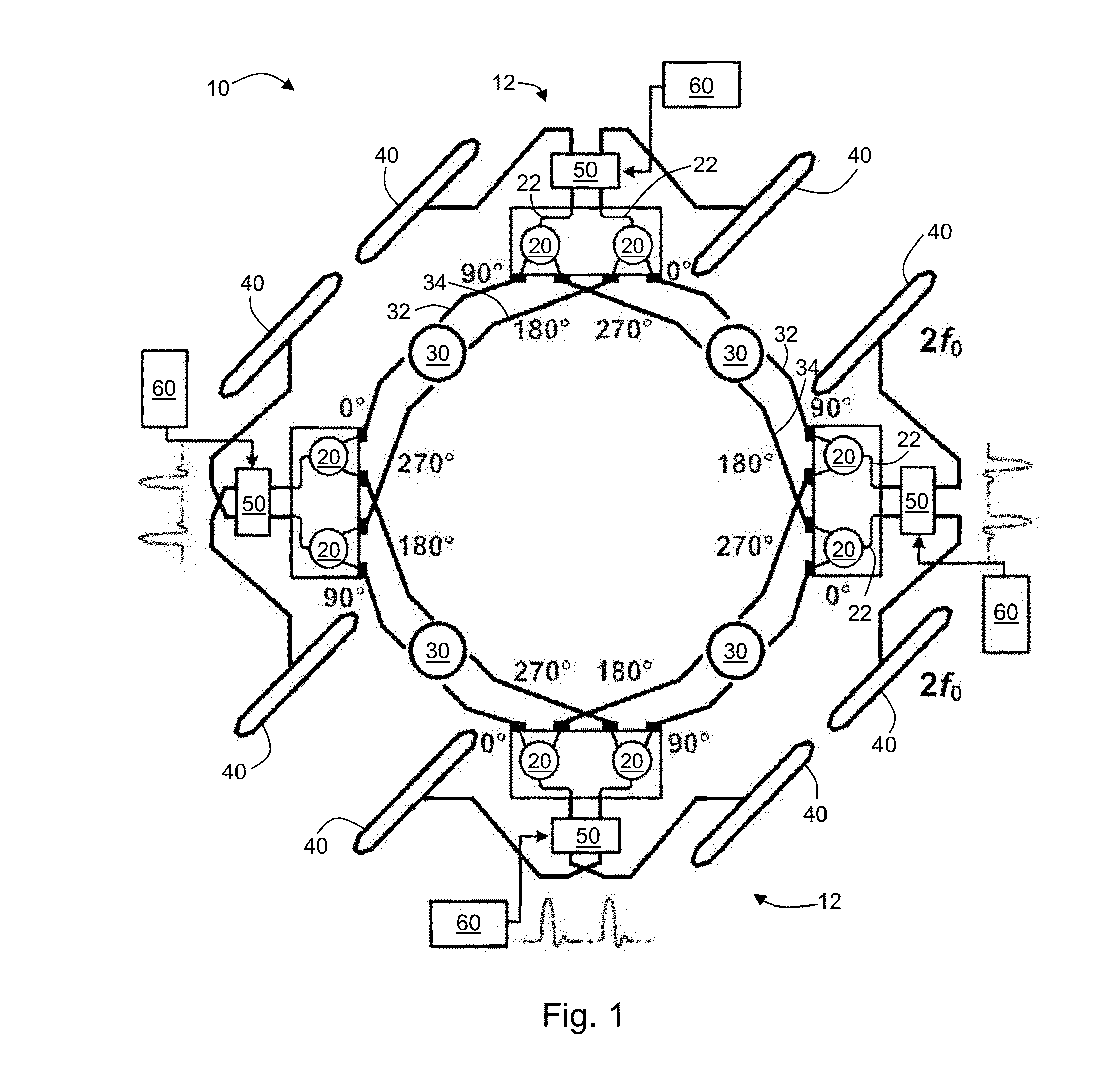
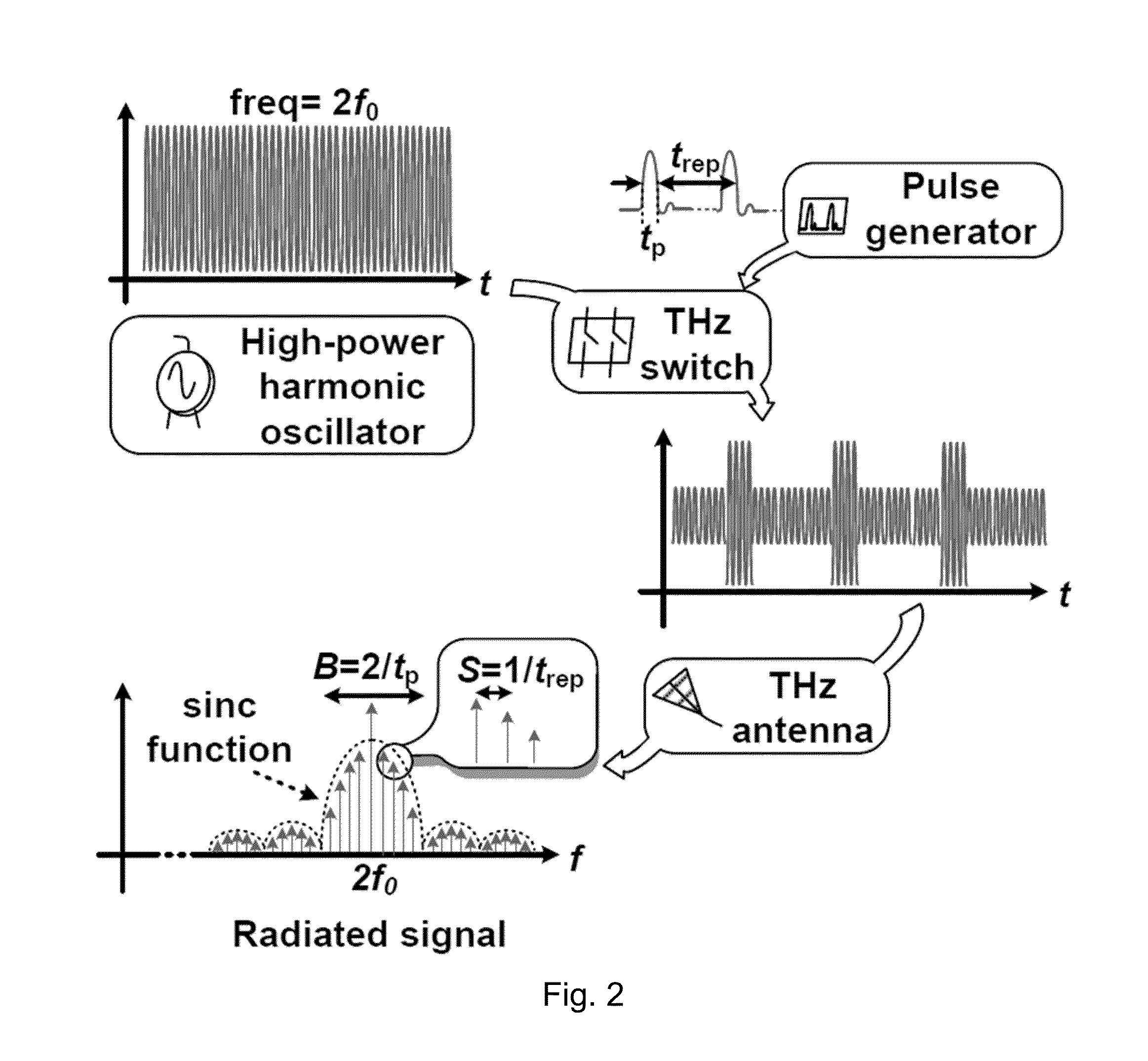
[0057]In an aspect of the present disclosure, embodiments of a high-power, sub-millimeter-wave radiation source are provided. In some embodiments, a 65-nm bulk CMOS technology may be used. The architecture of an exemplary transmitter 10 is shown in FIG. 1, where four differential core oscillator 20 pairs (radiator units) are mutually coupled through four quadrature oscillators 30. In an embodiment, each core oscillator pair operates at 130 GHz and generates 2nd-harmonic signals at 260 GHz that are power-combined after radiating through eight on-chip antennas 40. Embodiments may include four shunt switches 50, controlled by narrow pulses (width≈45 ps), to modulate the radiation. The pulses can be generated by local digital circuit blocks 60 with programmable repetition rate up to 5 GHz. In this way, the broadband spectrum of the pulses is up-converted to the carrier frequency of 260 GHz. Without modulation, the chip 10 achieves a continuous-wave radiated power of 1.1 mW. Under modula...


PUM


Abstract

A high-power broadband radiation system and method are disclosed. The system includes an array of harmonic oscillators with mutual coupling through quadrature oscillators. Based on a self-feeding structure, the presently disclosed harmonic oscillators simultaneously achieve optimum conditions for fundamental oscillation and 2nd-harmonic generation. The signals at the second harmonic radiate through on-chip slot antennas, and are in-phase combined inside a hemispheric silicon lens attached at the backside of the chip. In some embodiments, the radiation of the system can also be modulated by narrow pulses generated on chip, thereby achieving broad radiation bandwidth.

Description

CROSS-REFERENCE TO RELATED APPLICATIONS[0001]This application claims priority to U.S. Provisional Application No. 61 / 940,823, filed on Feb. 17, 2014, now pending, the disclosure of which is incorporated herein by reference.STATEMENT REGARDING FEDERALLY SPONSORED RESEARCH[0002]This invention was made with government support under contract no. 59980 / A001 awarded by the National Science Foundation and 65831 / A001 awarded by the Office of Naval Research. The government has certain rights in the invention.FIELD OF THE DISCLOSURE[0003]The disclosure relates to terahertz signal generation.BACKGROUND OF THE DISCLOSURE[0004]Terahertz spectroscopy using silicon technology is gaining attraction for future portable and affordable material identification equipment. To do this, a broadband THz radiation source is critical. Unfortunately, the bandwidth of the prior CMOS works is limited. In a previous design, a 300 GHz signal source achieves 4.5% tuning range by changing the coupling among multiple...

Claims


Application Information

Patent Timeline
IPC IPC(8): H04B1/04H04B7/06H04L27/04
CPCH04B1/0483H04B7/0602H04L27/04H04B1/04
Inventor HAN, RUONANAFSHARI, EHSAN
Owner CORNELL UNIVERSITY
Why Eureka
Try Eureka