Input and output device

a display device and input and output technology, applied in thermoelectric devices, solid-state devices, instruments, etc., can solve the problems of cracking, cracking, and a thin film in the end portion of the substrate that is difficult to separate and divide, and achieves high bending stress

Active Publication Date: 2015-10-29
SEMICON ENERGY LAB CO LTD
View PDF6 Cites 37 Cited by
  • Summary
  • Abstract
  • Description
  • Claims
  • Application Information

AI Technical Summary

Benefits of technology

[0011]In the case where peeling is performed between a separation layer provided over a substrate and a layer to be separated (hereinafter also referred to as a buffer layer) formed over the separation layer, a stack of thin films (e.g., the layer to be separated, a thin film transistor, a wiring, and an interlayer film) is provided over the separation layer. The stack has a thickness of several micrometers or less and is very fragile in some cases. When peeling is performed between the separation layer and the layer to be separated, a high bending stress is applied to an end portion of the substrate (a separation starting point); as a result, breaking or cracking (hereinafter, collectively referred to as a crack) easily occurs in the layer to be separated.
[0012]To improve the productivity of a flexible input and output device, it is preferable that a plurality of input and output devices be simultaneously manufactured over a large substrate and the substrate be divided with a scriber or the like. At this time, due to stress applied when the substrate is divided, a crack might occur in a thin film in an end portion of the substrate, particularly in the layer to be separated.
[0013]When the flexible light-emitting device that is manufactured in the aforementioned separating and dividing steps is held in a high temperature and high humidity environment, the crack, which occurs in the end portion of the layer to be separated in the separating and dividing steps, develops in some cases. The development of the crack reduces the reliability of light-emitting elements in the input and output device, or some of the light-emitting element emit no light because of the crack reaching the light-emitting elements.

Problems solved by technology

The stack has a thickness of several micrometers or less and is very fragile in some cases.
At this time, due to stress applied when the substrate is divided, a crack might occur in a thin film in an end portion of the substrate, particularly in the layer to be separated.
When the flexible light-emitting device that is manufactured in the aforementioned separating and dividing steps is held in a high temperature and high humidity environment, the crack, which occurs in the end portion of the layer to be separated in the separating and dividing steps, develops in some cases.
The development of the crack reduces the reliability of light-emitting elements in the input and output device, or some of the light-emitting element emit no light because of the crack reaching the light-emitting elements.

Method used


Image

  • Input and output device
  • Input and output device
  • Input and output device

Examples


embodiment 1

[0048]In Embodiment 1, an example of an input and output device (also referred to as input / output device) of one embodiment of the present invention is described. A structure and a manufacturing method of a touch panel in which an image display device is incorporated with an input device will be described with reference to drawings.

[0049]An example of the image display device in Embodiment 1 is a touch panel including an organic electroluminescence (EL) element.

[Structure Example of Touch Panel]

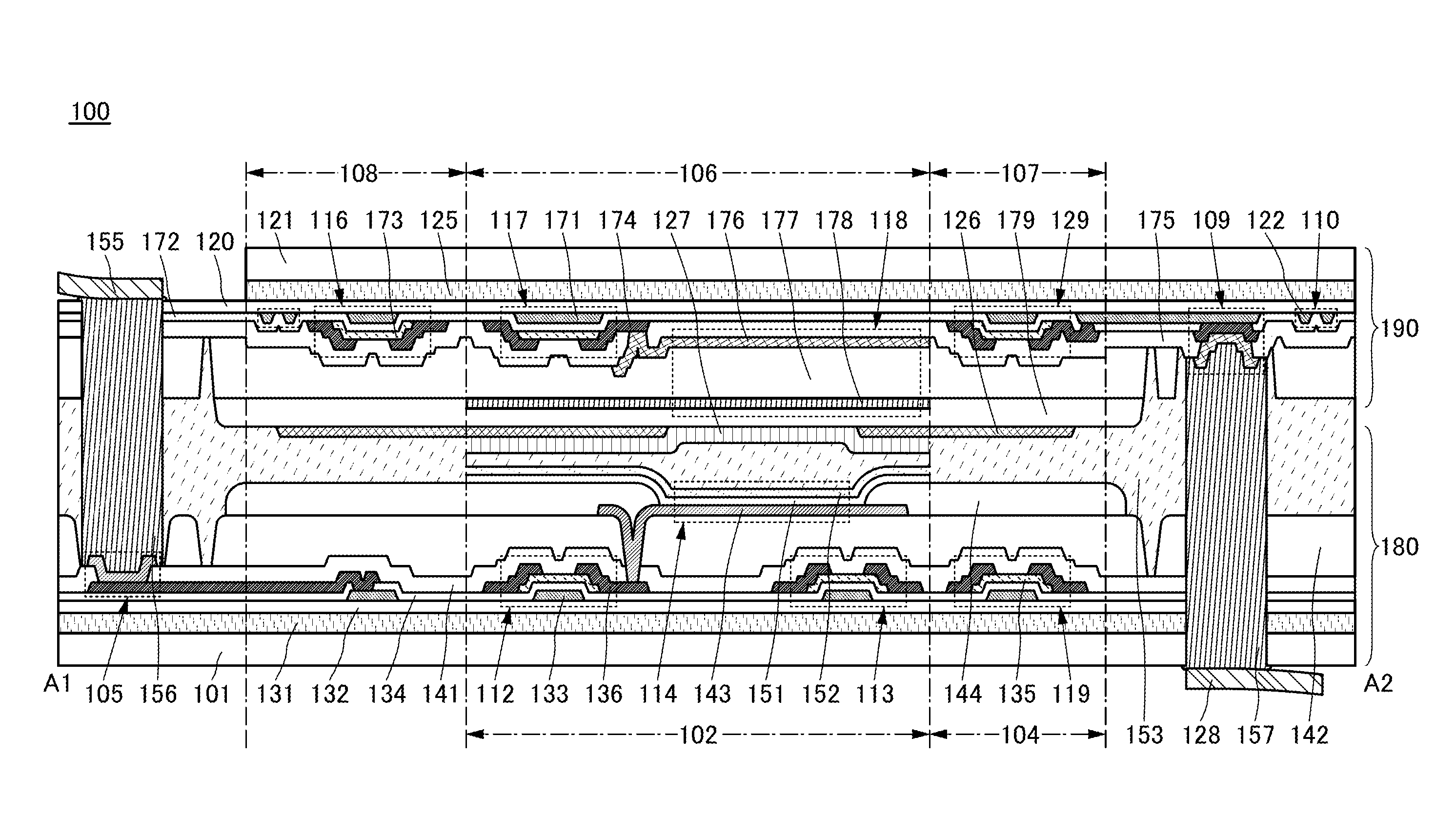
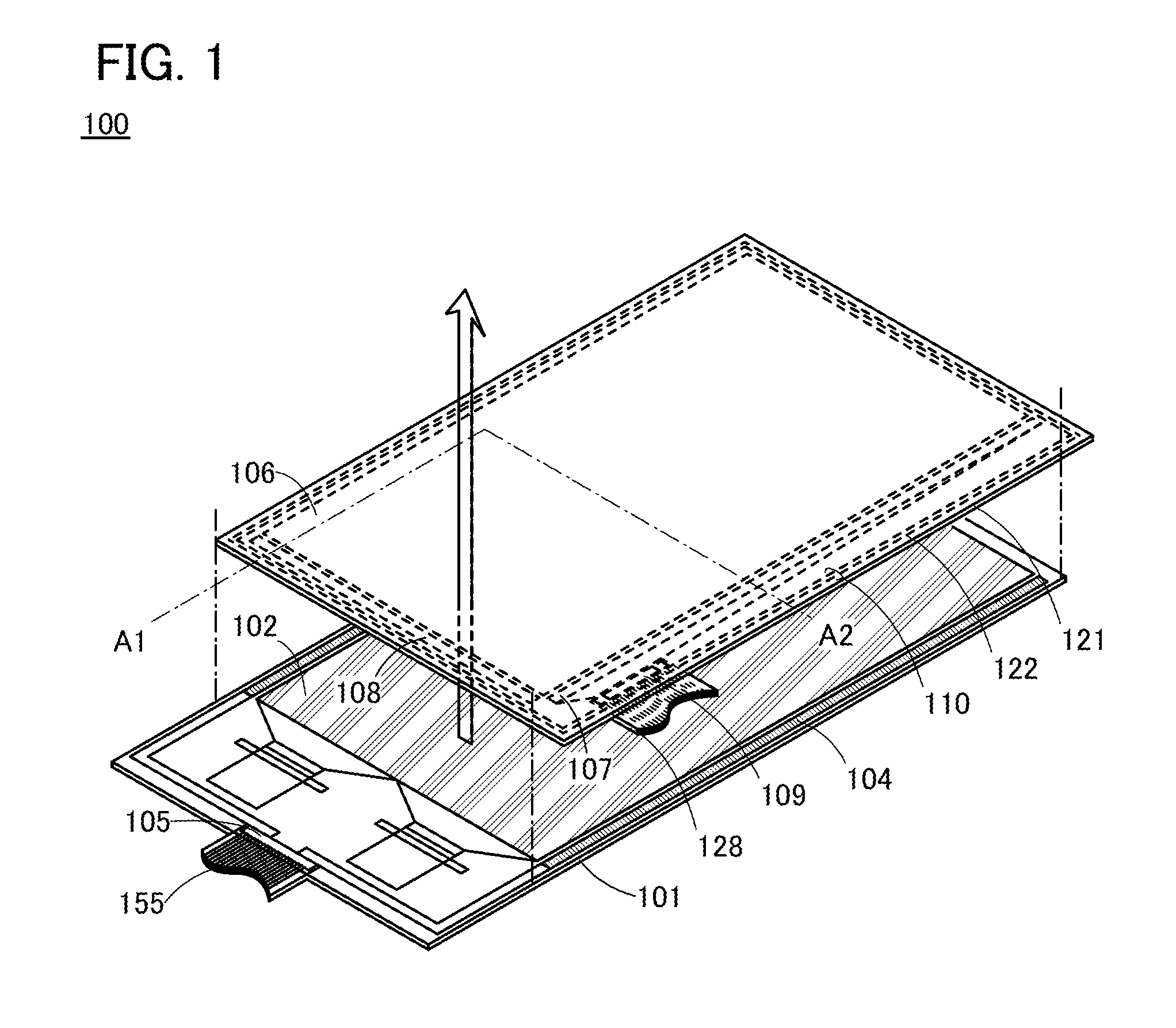
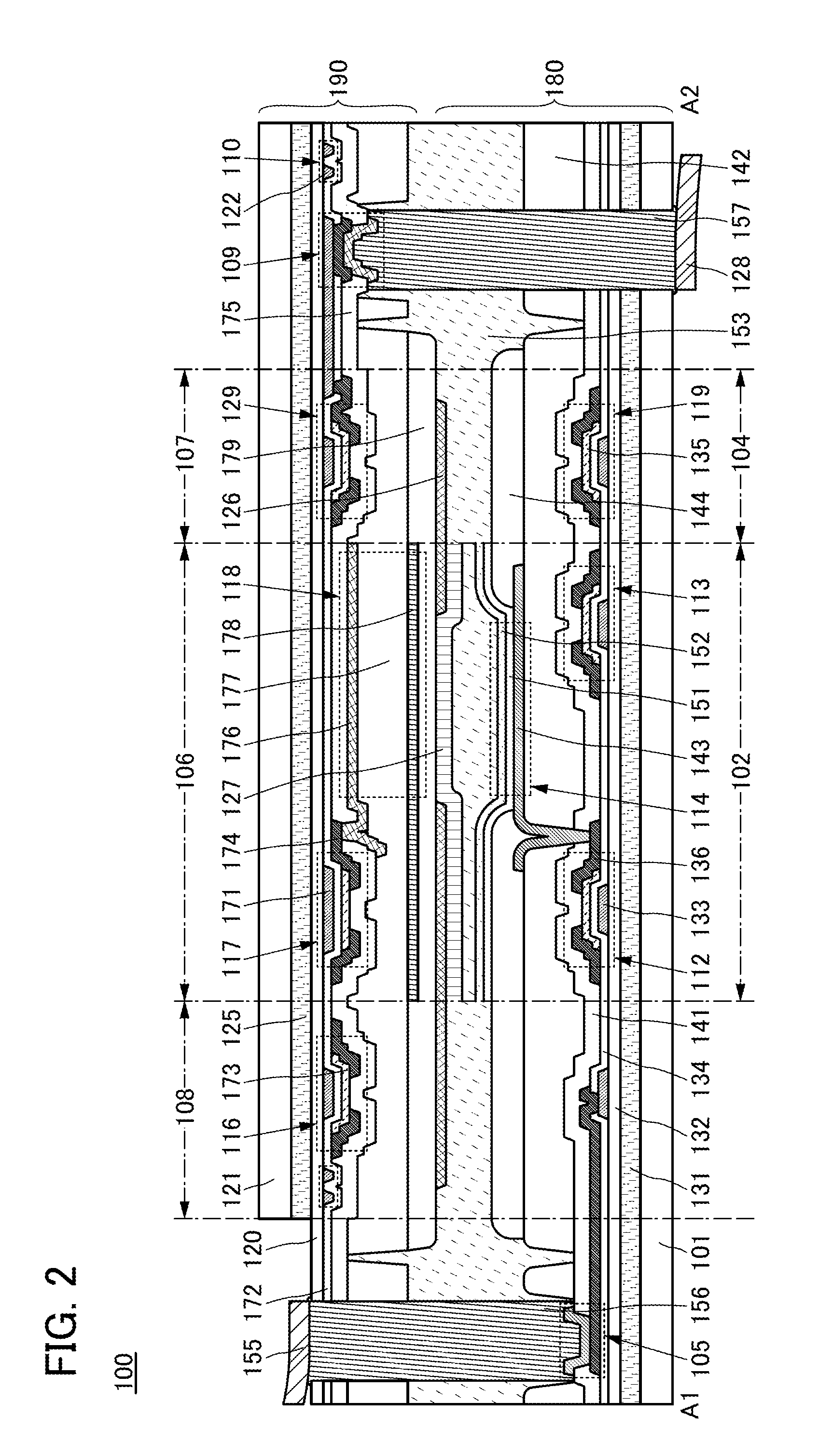
[0050]FIG. 1 is a projection view illustrating a structure of a touch panel 100 which is one embodiment of the present invention. FIG. 2 is a cross-sectional view of the touch panel 100 taken along dashed-dotted line A1-A2 in FIG. 1. Note that some components are not illustrated in FIG. 1 and FIG. 2 for clarity.

[0051]The touch panel 100 includes an image display device 180 and an input device 190 (see FIG. 2).

[0052]The touch panel 100 includes, on a surface of a first substrate 121 opposite t...

modification example 1

[Modification Example 1]

[0242]FIG. 9 is a cross-sectional schematic view of the touch panel 100 of one embodiment of the present invention in which one electrode of the sensor element 118 is formed in the same process as a semiconductor layer. The main differences of FIG. 9 from FIG. 2 are that two layers, an oxide semiconductor layer 173a and an oxide conductor layer 173b, are formed using an oxide semiconductor and that an insulating layer 175a is formed. The oxide semiconductor layer 173a includes a region functioning as a channel in the transistor in the input device 190. The oxide conductor layer 173b functions as one electrode of the sensor element 118. The differences from FIG. 2 will be described.

[0243]Note that in this specification and the like, the oxide conductor layer can also be referred to as an oxide semiconductor layer having a high carrier density and a low resistance, an oxide semiconductor layer having conductivity, an oxide semiconductor layer having high conduc...

modification example 2

[0262]FIG. 10 is a cross-sectional schematic view of the touch panel 100 of one embodiment of the present invention in which one electrode of the sensor element 118 is formed in the same process as a semiconductor layer. The main difference of FIG. 10 from FIG. 9 is that the conductive layer 178, which is the other electrode of a sensor element, is formed closer to the light-emitting element 114 than the color filer 127. The differences from FIG. 9 will be described.

[0263]The black matrix 126 and the color filter 127 are provided over the insulating layer 177. The conductive layer 178 is provided over the color filter 127 and the black matrix 126 with the insulating layer 179 therebetween. Note that the conductive layer 178 may be provided directly on the color filter 127 and the black matrix 126 without the insulating layer 179. An insulating layer may be provided over the conductive layer 178.

[0264]The conductive layer 178 is provided far from the oxide conductor layer 173b, which...


PUM


Abstract

A flexible input and output device in which defects due to a crack is reduced. The input and output device includes a first flexible substrate, a second flexible substrate, a first buffer layer, a first crack inhibiting layer, an input device, and a light-emitting element. A first surface of the first flexible substrate faces a second surface of the second flexible substrate. The first buffer layer, the first crack inhibiting layer, and the input device are provided on the first surface side of the first flexible substrate. The first buffer layer includes a region overlapping with the first crack inhibiting layer. The first buffer layer is between the first crack inhibiting layer and the first surface. The input device includes a transistor and a sensor element. The light-emitting element is provided on the second surface side of the second flexible substrate.

Description

BACKGROUND OF THE INVENTION[0001]1. Field of the Invention[0002]One embodiment of the present invention relates to a display device, and particularly to a flexible display device capable of performing display along a curved surface. One embodiment of the present invention relates to an input and output device and particularly to a flexible input and output device capable of performing display along a curved surface.[0003]Note that one embodiment of the present invention is not limited to the technical field. The technical field of one embodiment of the invention disclosed in this specification and the like relates to an object, a method, or a manufacturing method. One embodiment of the present invention relates to a process, a machine, manufacture, or a composition of matter. Specifically, the technical field of one embodiment of the present invention disclosed in this specification includes a semiconductor device, a display device, a light-emitting device, an electronic device, a m...

Claims


Application Information

Patent Timeline
Patent Type & Authority Applications(United States)
IPC IPC(8): H01L27/32H01L51/00
CPCH01L27/323H01L27/322H01L27/3272H01L51/0097G06F3/0412G06F3/0445H10K59/38H10K59/40H10K77/111H10K50/865H10K50/844H10K2102/311G06F15/0216G06F3/045
Inventor SENDA, NAOYUKINAKADA, MASATAKAABE, TAKAYUKIKUSUNOKI, KOJISHISHIDO, HIDEAKI
Owner SEMICON ENERGY LAB CO LTD
Why Eureka
Try Eureka